ZHCSH86B December   2017  – February 2019 LMH5401-SP

PRODUCTION DATA.  

  1. 特性
  2. 应用
  3. 说明
    1.     Device Images
      1.      LMH5401-SP 小信号频率响应
      2.      LMH5401-SP 驱动 ADC12D1620QML
  4. 修订历史记录
  5. 说明 (续)
  6. Pin Configuration and Functions
    1.     Pin Functions
  7. Specifications
    1. 7.1 Absolute Maximum Ratings
    2. 7.2 ESD Ratings
    3. 7.3 Recommended Operating Conditions
    4. 7.4 Thermal Information
    5. 7.5 Electrical Characteristics: VS = 5 V
    6. 7.6 Electrical Characteristics: VS = 3.3 V
    7. 7.7 Typical Characteristics: 5 V
    8. 7.8 Typical Characteristics: 3.3 V
  8. Parameter Measurement Information
    1. 8.1  Output Reference Nodes and Gain Nomenclature
    2. 8.2  ATE Testing and DC Measurements
    3. 8.3  Frequency Response
    4. 8.4  S-Parameters
    5. 8.5  Frequency Response with Capacitive Load
    6. 8.6  Distortion
    7. 8.7  Noise Figure
    8. 8.8  Pulse Response, Slew Rate, and Overdrive Recovery
    9. 8.9  Power Down
    10. 8.10 VCM Frequency Response
    11. 8.11 Test Schematics
  9. Detailed Description
    1. 9.1 Overview
    2. 9.2 Functional Block Diagram
    3. 9.3 Feature Description
      1. 9.3.1 Fully-Differential Amplifier
      2. 9.3.2 Operations for Single-Ended to Differential Signals
        1. 9.3.2.1 AC-Coupled Signal Path Considerations for Single-Ended Input to Differential Output Conversion
        2. 9.3.2.2 DC-Coupled Input Signal Path Considerations for SE-DE Conversions
        3. 9.3.2.3 Resistor Design Equations for Single-to-Differential Applications
        4. 9.3.2.4 Input Impedance Calculations
      3. 9.3.3 Differential-to-Differential Signals
        1. 9.3.3.1 AC-Coupled, Differential-Input to Differential-Output Design Issues
        2. 9.3.3.2 DC-Coupled, Differential-Input to Differential-Output Design Issues
      4. 9.3.4 Output Common-Mode Voltage
    4. 9.4 Device Functional Modes
      1. 9.4.1 Operation With a Split Supply
      2. 9.4.2 Operation With a Single Supply
  10. 10Application and Implementation
    1. 10.1 Application Information
      1. 10.1.1 Stability, Noise Gain, and Signal Gain
      2. 10.1.2 Input and Output Headroom Considerations
      3. 10.1.3 Noise Analysis
      4. 10.1.4 Noise Figure
      5. 10.1.5 Thermal Considerations
    2. 10.2 Typical Application
      1. 10.2.1 Design Requirements
      2. 10.2.2 Detailed Design Procedure
        1. 10.2.2.1 Driving Matched Loads
        2. 10.2.2.2 Driving Unmatched Loads For Lower Loss
        3. 10.2.2.3 Driving Capacitive Loads
        4. 10.2.2.4 Driving ADCs
          1. 10.2.2.4.1 SNR Considerations
          2. 10.2.2.4.2 SFDR Considerations
          3. 10.2.2.4.3 ADC Input Common-Mode Voltage Considerations—AC-Coupled Input
          4. 10.2.2.4.4 ADC Input Common-Mode Voltage Considerations—DC-Coupled Input
        5. 10.2.2.5 GSPS ADC Driver
        6. 10.2.2.6 Common-Mode Voltage Correction
        7. 10.2.2.7 Active Balun
      3. 10.2.3 Application Curves
    3. 10.3 Do's and Don'ts
      1. 10.3.1 Do:
      2. 10.3.2 Don't:
  11. 11Power Supply Recommendations
    1. 11.1 Supply Voltage
    2. 11.2 Single Supply
    3. 11.3 Split Supply
    4. 11.4 Supply Decoupling
  12. 12Layout
    1. 12.1 Layout Guidelines
    2. 12.2 Layout Example
  13. 13器件和文档支持
    1. 13.1 器件支持
      1. 13.1.1 器件命名规则
    2. 13.2 文档支持
      1. 13.2.1 相关文档
    3. 13.3 接收文档更新通知
    4. 13.4 社区资源
    5. 13.5 商标
    6. 13.6 静电放电警告
    7. 13.7 术语表
  14. 14机械、封装和可订购信息

封装选项

机械数据 (封装 | 引脚)
散热焊盘机械数据 (封装 | 引脚)
订购信息

Application Curves

The LMH5401-SP has on-chip series output resistors to isolate the output of the amplifier. These resistors provide the LMH5401-SP extra phase margin in most applications. When the amplifier is used to drive a terminated transmission line or a controlled impedance filter, additional external resistance is required to match the transmission line of the filter. In these matched applications, there is a 6-dB loss of gain. When the LMH5401-SP is used to drive loads that are not back-terminated or matched, there is a loss in gain resulting from the on-chip resistors. Figure 76 shows that loss for different load conditions. In most cases the loads are between 50 Ω and 200 Ω, where the on-chip resistor losses are 1.6 dB and 0.42 dB, respectively. As an example, if the LMH5401-SP were to drive an ADC with a differential input impedance of 100 Ω without any matching components the signal loss would be 0.83 dB compared to 6 dB in a matched configuration. Of course, this is only feasible if the LMH5401-SP and the ADC are placed in close proximity (< 1/4 wavelength of the frequency of interest) so as to avoid standing waves from reflections due to the mismatch in impedances). Figure 77 shows the net gain realized by the amplifier for a large range of load resistances when the LMH5401-SP is configured for 16-dB gain.
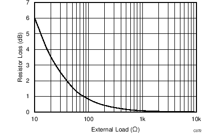
LMH5401-SP ai_C072_Gain_loss_bos695.pngFigure 76. Gain Loss Resulting from On-Chip Output Resistors
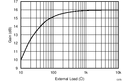
LMH5401-SP ai_C073_Gain_Load_bos695.pngFigure 77. Net Gain versus Load Resistance