ZHCSDQ5A April 2015 – May 2015 LMH6401
PRODUCTION DATA.
- 1 特性
- 2 应用
- 3 说明
- 4 修订历史记录
- 5 Device Options
- 6 Pin Configuration and Functions
- 7 Specifications
- 8 Parameter Measurement Information
-
9 Detailed Description
- 9.1 Overview
- 9.2 Functional Block Diagram
- 9.3 Feature Description
- 9.4 Device Functional Modes
- 9.5 Programming
- 9.6
Register Maps
- 9.6.1 Revision ID (address = 0h, Read-Only) [default = 03h]
- 9.6.2 Product ID (address = 1h, Read-Only) [default = 00h]
- 9.6.3 Gain Control (address = 2h) [default = 20h]
- 9.6.4 Reserved (address = 3h) [default = 8Ch]
- 9.6.5 Thermal Feedback Gain Control (address = 4h) [default = 27h]
- 9.6.6 Thermal Feedback Frequency Control (address = 5h) [default = 45h]
- 10Application and Implementation
- 11Power-Supply Recommendations
- 12Layout
- 13器件和文档支持
- 14机械、封装和可订购信息
9 Detailed Description
9.1 Overview
The LMH6401 is a very high-performance, differential I/O, digitally-controlled variable gain amplifier (DVGA). The device is optimized for radio frequency (RF), intermediate frequency (IF), or high-speed time-domain applications with 3-dB bandwidths up to 4.5 GHz. The device is ideal for dc- or ac-coupled applications requiring a variable gain stage when driving an analog-to-digital converter (ADC).
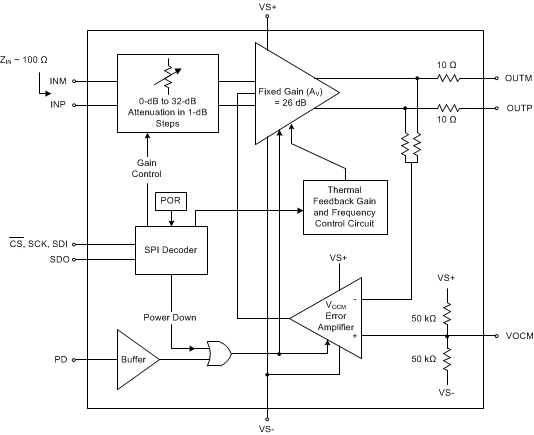
The LMH6401 is best suited to optimize system linearity and noise performance over the entire gain range in the RF and IF bands. Operating on a nominal 5-V supply or ±2.5-V split supplies, the device consists of an attenuator stage followed by a fixed-gain amplifier to provide voltage gain control from –6 dB to 26 dB in 1-dB steps (as shown in the Functional Block Diagram section) with an overall 32-dB gain range. The variable gain control for the device is offered through the digital serial peripheral interface (SPI) register. The device has a unique attenuator ladder architecture providing dynamic range improvements where the overall noise figure (NF) remains relatively constant for the first 5-dB attenuator steps, with NF degrading proportional to the attenuator steps on the sixth step. This behavior repeats over the entire gain range; see Figure 26.
The device has a differential input impedance of 100-Ω and is intended to be driven differentially by a matched 100-Ω differential source impedance for the best linearity and noise performance. The LMH6401 has two on-chip, 10-Ω resistors, one on each output (as shown in the Functional Block Diagram section). For most load conditions, the 10-Ω resistors are only a partial termination. Consequently, external termination resistors are required in most applications. See Table 11 for common load values and the matching resistors.
The LMH6401 supports a common-mode reference input (VOCM) pin to align the amplifier output common-mode with the subsequent stage (ADC) input requirements. The output common-mode of the LMH6401 is self-biased to mid-supply when the VOCM pin is not driven externally. The device can be operated on a power-supply voltage range of 4.0 V to 5.25 V and supports both single- and split-supply operation. For correct digital operation, the positive supply must not be below 2 V for ground reference logic. A power-down feature is also available through the SPI register and the external PD pin.
9.2 Functional Block Diagram

9.3 Feature Description
The LMH6401 includes the following features:
- Fully-differential amplifier
- Digitally-controlled variable gain: –6 dB to 26 dB in 1-dB steps
- Output common-mode control
- Single- or split-supply operation
- Large-signal bandwidth of 4.5 GHz
- Usable bandwidth up to 2 GHz
- Power-down control
9.4 Device Functional Modes
9.4.1 Power-On Reset (POR)
The LMH6401 has a built-in, power-on reset (POR) that sets the device registers to their default state (see Table 3) on power-up. Note that the LMH6401 register information is lost each time power is removed. When power is reapplied, the POR ensures the device enters a default state. Power glitches (of sufficient duration) can also initiate the POR and return the device to a default state.
9.4.2 Power-Down (PD)
The device supports power-down control using an external power-down (PD) pin or by writing a logic high to bit 6 of SPI register 2h (see the Register Maps section). The external PD is an active high pin. When left floating, the device defaults to an on condition when the PD pin defaults to logic low as a result of the internal pulldown resistor. The device PD thresholds are noted in the Electrical Characteristics table. The device consumes approximately 7 mA in power-down mode. Note that the SPI register contents are preserved in power-down mode.
9.4.3 Thermal Feedback Control
The LMH6401 has a thermal feedback gain and frequency control feature that allows for improved low-frequency settling performance. The Thermal Feedback Gain Control and Thermal Feedback Frequency Control registers set through the SPI control this feature. The default setting is described in Table 3. Graphs are Included in the Application and Implementation section that illustrate how the thermal feedback gain and frequency control allows for enhanced performance.
9.4.4 Gain Control
The LMH6401 gain can be controlled from 26-dB gain (0-dB attenuation) to –6-dB gain in 1-dB steps by digitally programming the SPI register 2h. See the Register Maps section for more details.
9.5 Programming
9.5.1 Details of the Serial Interface
The LMH6401 has a set of internal registers that can be accessed by the serial interface controlled by the CS (chip select), SCLK (serial interface clock), SDI (serial interface input data), and SDO (serial interface readback data) pins. Serial input to the device is enabled when CS is low. SDI serial data are latched at every SCLK rising edge when CS is active (low). Serial data are loaded into the register at every 16th SCLK rising edge when CS is low. When the word length exceeds a multiple of 16 bits, the excess bits are ignored. Data can be loaded in multiples of 16-bit words within a single active CS pulse. The first eight bits form the register address and the remaining eight bits form the register data. The interface can function with SCLK frequencies from 50 MHz down to very low speeds (of a few Hertz) and also with a non-50% SCLK duty cycle. A summary of the LMH6401 SPI protocol follows:
- SPI-1.1 compliant interface
- SPI register contents protected in power-down
- SPI-controlled power-down
- Powered from the main VS+ power supply
- 1.8-V logic compliant
9.5.2 Timing Diagrams
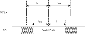
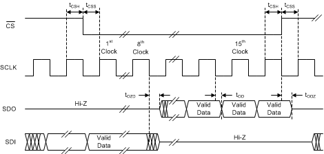
Figure 47 and Figure 48 show timing diagrams for the SPI write and read bus cycles, respectively. Figure 49 and Figure 50 show timing diagrams for the write and read operations, respectively, of the LMH6401. Figure 51 and Figure 52 illustrate example SPI stream write and read timing diagrams, respectively. Refer to the Electrical Characteristics table for SPI timing requirements.
 Figure 47. SPI Write Bus Cycle
 Figure 48. SPI Read Bus Cycle
 Figure 49. Write Operation Timing Diagram
 Figure 50. Read Operation Timing Diagram
 Figure 51. SPI Streaming Write Example
 Figure 52. SPI Streaming Read Example
9.6 Register Maps
Table 3 lists the SPI register map.
Table 3. SPI Register Map
| ADDRESS (A[6:0]) |
R/W | REGISTER | DEFAULT (Hex) |
|---|---|---|---|
| 0 | R | Revision ID | 03h |
| 1 | R | Product ID | 00h |
| 2 | R/W | Gain Control | 20h (minimum gain) |
| 3 | R/W | Reserved | 8Ch |
| 4 | R/W | Thermal feedback gain control | 27h |
| 5 | R/W | Thermal feedback frequency control | 45h |
| 6-127 | R | Reserved | 00h |
9.6.1 Revision ID (address = 0h, Read-Only) [default = 03h]
| 7 | 6 | 5 | 4 | 3 | 2 | 1 | 0 |
| Revision ID | |||||||
| R-0b | R-0b | R-0b | R-0b | R-0b | R-0b | R-1b | R-1b |
| LEGEND: R = Read only; -n = value after reset |
Table 4. Revision ID Field Descriptions
| Bit | Field | Type | Default | Description |
|---|---|---|---|---|
| 7-0 | Revision ID | R | 00000011 | Revision identification bits. |
9.6.2 Product ID (address = 1h, Read-Only) [default = 00h]
| 7 | 6 | 5 | 4 | 3 | 2 | 1 | 0 |
| Product ID | |||||||
| R-0b | R-0b | R-0b | R-0b | R-0b | R-0b | R-0b | R-0b |
| LEGEND: R = Read only; -n = value after reset |
Table 5. Product ID Field Descriptions
| Bit | Field | Type | Default | Description |
|---|---|---|---|---|
| 7-0 | Product ID | R | 00000000 | Product identification bits. |
9.6.3 Gain Control (address = 2h) [default = 20h]
| 7 | 6 | 5 | 4 | 3 | 2 | 1 | 0 |
| Reserved | Power Down | Gain Control | |||||
| R/W-0b | R/W-0b | R/W-1b | R/W-0b | R/W-0b | R/W-0b | R/W-0b | R/W-0b |
| LEGEND: R/W = Read/Write; -n = value after reset |
Table 6. Gain Control Field Description
| Bit | Field | Type | Default | Description |
|---|---|---|---|---|
| 7 | Reserved | R/W | 0 | Reserved, always program to 0 |
| 6 | Power Down | R/W | 0 | 0 = Active 1 = Power down |
| 5-0 | Gain Control | R/W | 100000 | Gain control (see Table 10 for gain settings) |
9.6.4 Reserved (address = 3h) [default = 8Ch]
| 7 | 6 | 5 | 4 | 3 | 2 | 1 | 0 |
| Reserved | |||||||
| R/W-1b | R/W-0b | R/W-0b | R/W-0b | R/W-1b | R/W-1b | R/W-0b | R/W-0b |
| LEGEND: R/W = Read/Write; -n = value after reset |
Table 7. Reserved Field Descriptions
| Bit | Field | Type | Default | Description |
|---|---|---|---|---|
| 7-0 | Reserved | R/W | 10001100 | Reserved |
9.6.5 Thermal Feedback Gain Control (address = 4h) [default = 27h]
| 7 | 6 | 5 | 4 | 3 | 2 | 1 | 0 |
| Reserved | Reserved | Thermal SD | Thermal Feedback Gain Control | ||||
| R/W-0b | R/W-0b | R/W-1b | R/W-0b | R/W-0b | R/W-1b | R/W-1b | R/W-1b |
| LEGEND: R/W = Read/Write; -n = value after reset |
Table 8. Thermal Feedback Gain Control Field Descriptions
| Bit | Field | Type | Default | Description |
|---|---|---|---|---|
| 7-6 | Reserved | R/W | 00 | Reserved, always program to 00 |
| 5 | Thermal SD | R/W | 1 | 0 = Thermal feedback control enabled 1 = Thermal feedback control disabled |
| 4-0 | Thermal Feedback Gain Control | R/W | 00111 | 00000 = Minimum thermal feedback gain (see Figure 61) 11111 = Maximum thermal feedback gain (see Figure 61) |
9.6.6 Thermal Feedback Frequency Control (address = 5h) [default = 45h]
| 7 | 6 | 5 | 4 | 3 | 2 | 1 | 0 |
| Reserved | Reserved | Reserved | Thermal Feedback Frequency Control | ||||
| R/W-0b | R/W-1b | R/W-0b | R/W-0b | R/W-0b | R/W-1b | R/W-0b | R/W-1b |
| LEGEND: R/W = Read/Write; -n = value after reset |
Table 9. Thermal Feedback Frequency Control Field Descriptions
| Bit | Field | Type | Default | Description |
|---|---|---|---|---|
| 7-5 | Reserved | R/W | 010 | Reserved, always program to 010 |
| 4-0 | Thermal Feedback Frequency Control | R/W | 00101 | 00000 = Minimum thermal feedback frequency (see Figure 62) 11111 = Maximum thermal feedback frequency (see Figure 62) |
Table 10. Gain Control Register Controls
| ATTENUATION (dB) | GAIN (dB) | REGISTER SETTING (Address = 02h) |
|---|---|---|
| 0 | 26 | 00h |
| 1 | 25 | 01h |
| 2 | 24 | 02h |
| 3 | 23 | 03h |
| 4 | 22 | 04h |
| 5 | 21 | 05h |
| 6 | 20 | 06h |
| 7 | 19 | 07h |
| 8 | 18 | 08h |
| 9 | 17 | 09h |
| 10 | 16 | 0Ah |
| 11 | 15 | 0Bh |
| 12 | 14 | 0Ch |
| 13 | 13 | 0Dh |
| 14 | 12 | 0Eh |
| 15 | 11 | 0Fh |
| 16 | 10 | 10h |
| 17 | 9 | 11h |
| 18 | 8 | 12h |
| 19 | 7 | 13h |
| 20 | 6 | 14h |
| 21 | 5 | 15h |
| 22 | 4 | 16h |
| 23 | 3 | 17h |
| 24 | 2 | 18h |
| 25 | 1 | 19h |
| 26 | 0 | 1Ah |
| 27 | –1 | 1Bh |
| 28 | –2 | 1Ch |
| 29 | –3 | 1Dh |
| 30 | –4 | 1Eh |
| 31 | –5 | 1Fh |
| 32 | –6 | 20h-3Fh |