ZHCSDQ5A April 2015 – May 2015 LMH6401
PRODUCTION DATA.
- 1 特性
- 2 应用
- 3 说明
- 4 修订历史记录
- 5 Device Options
- 6 Pin Configuration and Functions
- 7 Specifications
- 8 Parameter Measurement Information
-
9 Detailed Description
- 9.1 Overview
- 9.2 Functional Block Diagram
- 9.3 Feature Description
- 9.4 Device Functional Modes
- 9.5 Programming
- 9.6
Register Maps
- 9.6.1 Revision ID (address = 0h, Read-Only) [default = 03h]
- 9.6.2 Product ID (address = 1h, Read-Only) [default = 00h]
- 9.6.3 Gain Control (address = 2h) [default = 20h]
- 9.6.4 Reserved (address = 3h) [default = 8Ch]
- 9.6.5 Thermal Feedback Gain Control (address = 4h) [default = 27h]
- 9.6.6 Thermal Feedback Frequency Control (address = 5h) [default = 45h]
- 10Application and Implementation
- 11Power-Supply Recommendations
- 12Layout
- 13器件和文档支持
- 14机械、封装和可订购信息
7 Specifications
7.1 Absolute Maximum Ratings
over operating free-air temperature range (unless otherwise noted)(1)| MIN | MAX | UNIT | ||
|---|---|---|---|---|
| Supply voltage | V = (VS+) – (VS–) | 5.5 | V | |
| Digital input pins | –0.3 | VS+ | V | |
| Maximum input difference voltage | 2.1 | V | ||
| Maximum input voltage | VS– | VS+ | V | |
| Temperature | Maximum junction, TJ | 150 | °C | |
| Maximum junction, continuous operation, long-term reliability | 125 | °C | ||
| Operating free-air, TA | –40 | 85 | °C | |
| Storage, Tstg | –65 | 150 | °C | |
(1) Stresses beyond those listed under Absolute Maximum Ratings may cause permanent damage to the device. These are stress ratings only, which do not imply functional operation of the device at these or any other conditions beyond those indicated under Recommended Operating Conditions. Exposure to absolute-maximum-rated conditions for extended periods may affect device reliability.
7.2 ESD Ratings
| VALUE | UNIT | |||
|---|---|---|---|---|
| V(ESD) | Electrostatic discharge | Human-body model (HBM), per ANSI/ESDA/JEDEC JS-001(1) | ±2000 | V |
| Charged-device model (CDM), per JEDEC specification JESD22-C101(2) | ±1000 | |||
(1) JEDEC document JEP155 states that 500-V HBM allows safe manufacturing with a standard ESD control process.
(2) JEDEC document JEP157 states that 250-V CDM allows safe manufacturing with a standard ESD control process.
7.3 Recommended Operating Conditions
over operating free-air temperature range (unless otherwise noted)| MIN | NOM | MAX | UNIT | ||
|---|---|---|---|---|---|
| Supply voltage | 4.0 | 5.0 | 5.25 | V | |
| Minimum operating positive (VS+) supply voltage | 2.0 | V | |||
| Ambient operating air temperature, TA | –40 | 25 | 85 | °C | |
| Operating junction temperature, TJ | –40 | 125 | °C | ||
7.4 Thermal Information
| THERMAL METRIC(1) | LMH6401 | UNIT | |
|---|---|---|---|
| RMZ (UQFN) | |||
| 16 PINS | |||
| RθJA | Junction-to-ambient thermal resistance | 78 | °C/W |
| RθJC(top) | Junction-to-case (top) thermal resistance | 43 | °C/W |
| RθJB | Junction-to-board thermal resistance | 24 | °C/W |
| ψJT | Junction-to-top characterization parameter | 2.3 | °C/W |
| ψJB | Junction-to-board characterization parameter | 24 | °C/W |
| RθJC(bot) | Junction-to-case (bottom) thermal resistance | n/a | °C/W |
(1) For more information about traditional and new thermal metrics, see the IC Package Thermal Metrics application report, SPRA953.
7.5 Electrical Characteristics
At TA = 25°C, VS– = –2.5 V, VS+ = 2.5 V, VOCM = 0 V, RLOAD = 200-Ω differential (Ro(internal, diff) = 20 Ω), VO = 2 VPPD, and AV = 26 dB, unless otherwise noted.| PARAMETER | TEST CONDITIONS | MIN | TYP | MAX | UNIT | TEST LEVEL(1) |
||
|---|---|---|---|---|---|---|---|---|
| DYNAMIC PERFORMANCE | ||||||||
| SSBW | Small-signal, –3-dB bandwidth | AV = 26 dB, VO = 200 mVPPD | 4.5 | GHz | C | |||
| LSBW | Large-signal, –3-dB bandwidth | AV = 26 dB, VO = 2.0 VPPD | 4.5 | GHz | C | |||
| Bandwidth for 0.1-dB flatness | AV = 26 dB, VO = 2.0 VPPD | 500 | MHz | C | ||||
| SR | Slew rate | VO = 2-V step | 18200 | V/µs | C | |||
| tR, tF | Rise and fall time | VO = 2-V step, 10% to 90% | 82 | ps | C | |||
| Overdrive recovery | Overdrive = ±0.5 V | 600 | ps | C | ||||
| Output balance error | f = 1 GHz | –47 | dB | C | ||||
| ts | Settling time to 1% | VO = 2-V step, RL= 200 Ω | 700 | ps | C | |||
| HD2 | Second-harmonic distortion | f = 200 MHz, VO = 2.0 VPPD | –73 | dBc | C | |||
| f = 500 MHz, VO = 2.0 VPPD | –68 | dBc | C | |||||
| f = 1 GHz, VO = 2.0 VPPD | –63 | dBc | C | |||||
| f = 2 GHz, VO = 2.0 VPPD | –58 | dBc | C | |||||
| HD3 | Third-harmonic distortion | f = 200 MHz, VO = 2.0 VPPD | –80 | dBc | C | |||
| f = 500 MHz, VO = 2.0 VPPD | –72 | dBc | C | |||||
| f = 1 GHz, VO = 2.0 VPPD | –63 | dBc | C | |||||
| f = 2 GHz, VO = 2.0 VPPD | –54 | dBc | C | |||||
| OIP2 | Output second-order intercept point | f = 200 MHz, PO = –2 dBm per tone | 67 | dBm | C | |||
| f = 500 MHz, PO = –2 dBm per tone | 65 | dBm | C | |||||
| f = 1 GHz, PO = –2 dBm per tone | 60 | dBm | C | |||||
| f = 2 GHz, PO = –2 dBm per tone | 52 | dBm | C | |||||
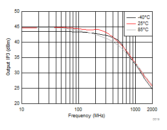
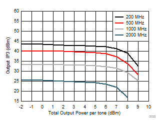
| OIP3 | Output third-order intercept point | f = 200 MHz, PO = –2 dBm per tone | 43 | dBm | C | |||
| f = 500 MHz, PO = –2 dBm per tone | 40 | dBm | C | |||||
| f = 1 GHz, PO = –2 dBm per tone | 33 | dBm | C | |||||
| f = 2 GHz, PO = –2 dBm per tone | 27 | dBm | C | |||||
| IMD2 | Second-order intermodulation distortion | f = 500 MHz, VO = 1.0 VPP per tone | –68 | dBc | C | |||
| IMD3 | Third-order intermodulation distortion | f = 500 MHz, VO = 1.0 VPP per tone | –83 | dBc | C | |||
| P1dB | 1-dB compression point | f = 500 MHz, power measured at amplifier output | 18.3 | dBm | C | |||
| NF | Noise figure | RS = 100 Ω | f = 200 MHz | 7.7 | dB | C | ||
| f = 1 GHz | 8 | dB | C | |||||
| Output-referred noise voltage | AV = 26 dB, f > 1 MHz | 30.4 | nV/√Hz | C | ||||
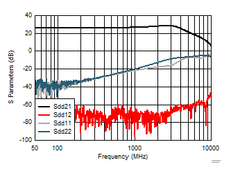
| S12 | Reverse transmission (S12) | f = 1 GHz | –65 | dB | C | |||
| S11 | Input return loss (S11) | 100-Ω system, f = 2 GHz | –15 | dB | C | |||
| GAIN PARAMETERS | ||||||||
| Maximum voltage gain | 25.5 | 26.0 | 26.5 | dB | A | |||
| Minimum voltage gain | –7.5 | –6.0 | –4.5 | dB | A | |||
| Gain range | 32 | dB | C | |||||
| Gain step size | 0.9 | 1 | 1.1 | dB | A | |||
| Cumulative gain error | AV = 26 dB to 10 dB (referenced to 26-dB gain) |
–0.5 | 0.5 | dB | A | |||
| AV = 26 dB to –6 dB (referenced to 26-dB gain) |
–1 | 1 | dB | A | ||||
| Gain step transition time | 1 | ns | C | |||||
| ANALOG INPUT CHARACTERISTICS | ||||||||
| Ri | Input resistance | Differential | 85 | 100 | 112 | Ω | A | |
| Ci | Input capacitance | Differential | 0.8 | pF | C | |||
| VICM | Input common-mode voltage | Self-biased to mid-supply | –0.3 | 0.3 | V | A | ||
| VICLR | Low-level input common-mode voltage range | Differential gain shift < 1 dB | (VS–) + 1.5 | V | C | |||
| VICHR | High-level input common-mode voltage range | Differential gain shift < 1 dB | (VS+) – 1.5 | V | C | |||
| ANALOG OUTPUT CHARACTERISTICS | ||||||||
| Ro | Output resistance | Differential | 18 | 20 | 25 | Ω | A | |
| VOL | Low-level output voltage range | Low-level clipping level | (VS–) + 1 | (VS–) + 1.1 | V | A | ||
| VOH | High-level output voltage range | High-level clipping level | (VS+) – 1.1 | (VS+) – 1 | V | A | ||
| VOM | Maximum output voltage swing | Differential | 6.0 | VPPD | C | |||
| CMRR | Common-mode rejection ratio | ±0.3-V input common-mode shift | 38.4 | 45 | dB | A | ||
| POWER SUPPLY | ||||||||
| VS | Supply voltage [V = (VS+) – (VS–)] | 4.0 | 5.0 | 5.25 | V | A | ||
| Minimum positive (VS+) supply voltage | 2.0 | V | A | |||||
| PSRR | Power-supply rejection ratio | VS–, measured at 1-kHz sine-wave | 66 | 70 | dB | A | ||
| VS+, measured at 1-kHz sine-wave | 66 | 70 | dB | A | ||||
| IQ | Quiescent current | PD = 0 (device enabled) | 60 | 69 | 78 | mA | A | |
| PD = 1 (device disabled) | 1 | 7 | 12 | mA | A | |||
| OUTPUT COMMON-MODE CONTROL (VOCM Pin) | ||||||||
| SSBW | Small-signal bandwidth | VOCM = 200 mVPP | 160 | MHz | C | |||
| VOCM voltage range low | VOCM gain < 2% | –0.5 | V | A | ||||
| VOCM voltage range high | VOCM gain < 2% | 0.5 | V | A | ||||
| VOO | Output offset voltage | All gain settings | –40 | 40 | mV | A | ||
| VOCM gain | 1.0 | V | C | |||||
| VOCM | Common-mode offset voltage | VOCM pin driven to GND | –10 | 10 | mV | A | ||
| POWER DOWN (PD Pin) | ||||||||
| Power-down quiescent current | 1 | 7 | 12 | mA | A | |||
| PD bias current | PD = 2.5 V | 80 | 100 | µA | A | |||
| Turn-on time delay | Time to VO = 90% of final value | 70 | ns | C | ||||
| Turn-off time delay | Time to VO = 10% of original value | 10 | ns | C | ||||
| DIGITAL INPUT/OUTPUT | ||||||||
| VIH | High-level input voltage | Referred to GND | 1.2 | VS+ | V | A | ||
| VIL | Low-level input voltage | Referred to GND | 0.8 | V | A | |||
| VOH | High-level output voltage | 1 kΩ to GND | 1.4 | V | A | |||
| VOL | Low-level output voltage | 1 kΩ to GND | 0.4 | V | A | |||
(1) Test levels: (A) 100% DC tested at 25°C unless otherwise specified. Over-temperature limits by characterization and simulation. (B) Limits set by bench verification and simulation. (C) Typical value only for information.
(2) Ensured by design.
(3) Reference to negative edge of SCLK.
(4) Reference to positive edge of SCLK.
7.6 SPI Timing Requirements(2)
At TA = 25°C, VS– = –2.5 V, VS+ = 2.5 V, VOCM = 0 V, RLOAD = 200-Ω differential (Ro(internal, diff) = 20 Ω), VO = 2 VPPD, and AV = 26 dB, unless otherwise noted. Limits set by bench verification and simulation.| MIN | NOM | MAX | UNIT | ||
|---|---|---|---|---|---|
| fs_c | SCLK frequency | 50 | MHz | ||
| tPH | SCLK pulse duration, high | 10 | ns | ||
| tPL | SCLK pulse duration, low | 10 | ns | ||
| tSU | SDI setup | 3 | ns | ||
| tH | SDO hold | 3 | ns | ||
| tIZ | SDO tri-state | 3 | ns | ||
| tODZ | SDO driven to tri-state(3) | 5 | ns | ||
| tOZD | SDO tri-state to driven | 3 | ns | ||
| tOD | SDO output delay(3) | 3 | ns | ||
| tCSS | CS setup(4) | 3 | ns | ||
| tCSH | CS hold | 3 | ns | ||
| tIAG | Inter-access gap | 20 | ns | ||
7.7 Typical Characteristics
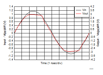
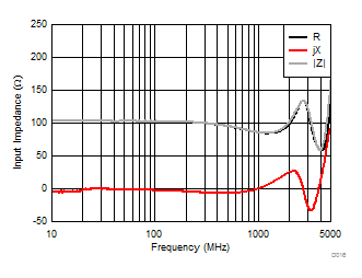
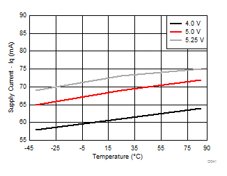
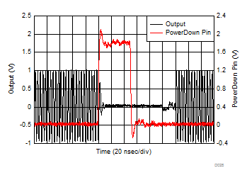
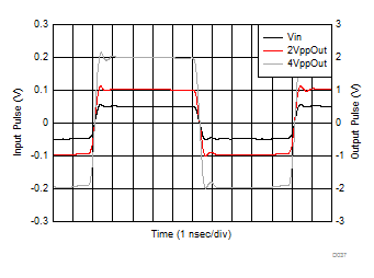
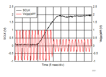
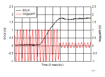
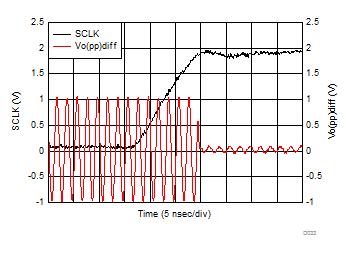
At TA = 25°C, VS– = –2.5 V, VS+ = 2.5 V, VOCM = 0 V, RLOAD = 200-Ω differential (Ro(internal, diff) = 20 Ω), VO = 2 VPPD, and AV = 26 dB, unless otherwise noted. Differential input and output, and input and output pins referenced to mid-supply, unless otherwise noted. Measured using an EVM as discussed in the Parameter Measurement Information section.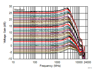
| PO = –2 dBm per tone |
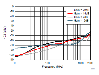
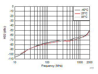
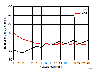
| f = 500 MHz |
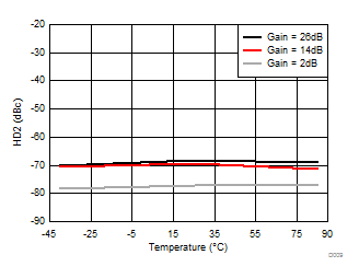
| f = 500 MHz |
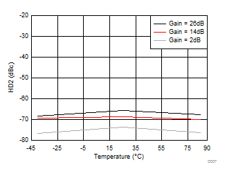
| f = 500 MHz, (VS+) – (VS–) = 4 V |
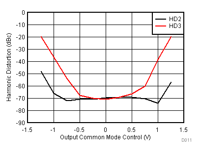
| f = 500 MHz |
Output Common-Mode Voltage
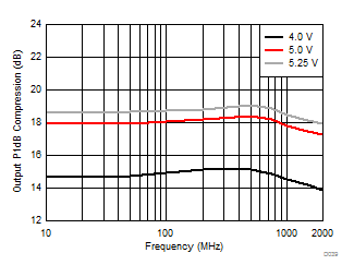
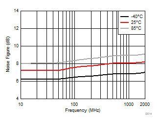
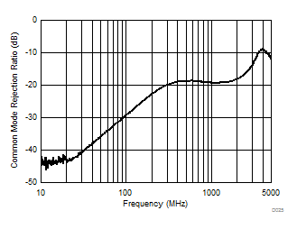
| Scc21 / Sdd21 |
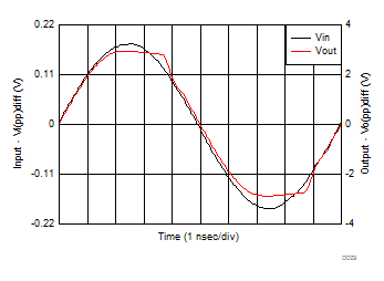
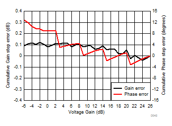
| f = 500 MHz |
Gain Settings
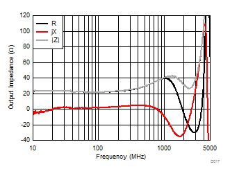
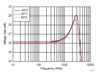
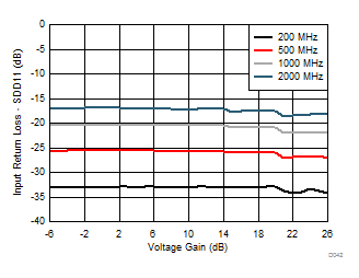
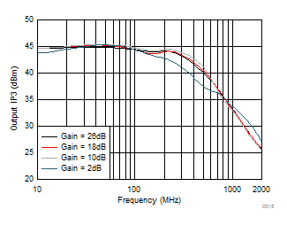
| PO = –2 dBm per tone |
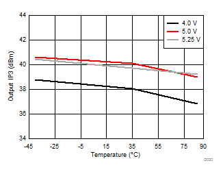
| f = 500 MHz, PO = –2 dBm per tone |
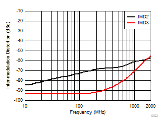
| PO = –2 dBm per tone |
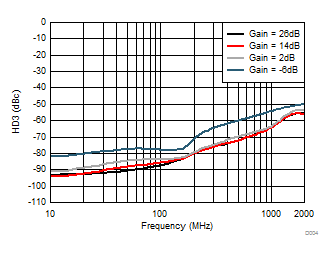
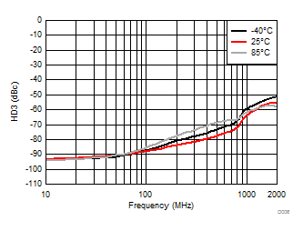
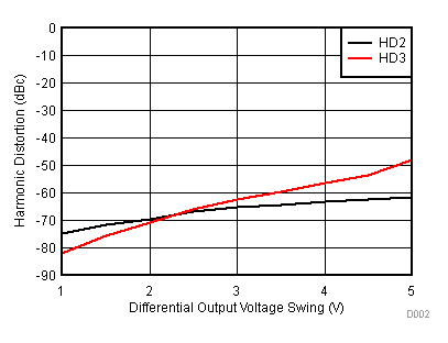
| f = 500 MHz |
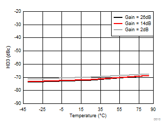
| f = 500 MHz |
Temperature
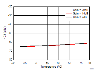
| f = 500 MHz, (VS+) – (VS–) = 4 V |
Temperature
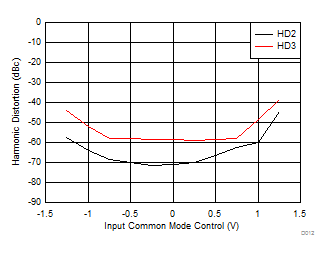
| f = 500 MHz, gain = –6 dB |
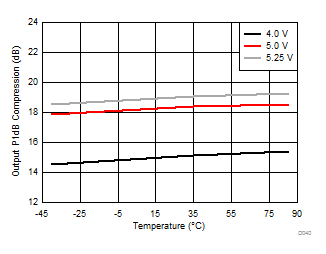
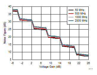
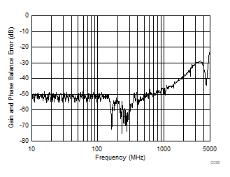
| Sdc21/Sdd21 |
