ZHCSGX2E May 2011 – August 2016 LMH6521
PRODUCTION DATA.
- 1 特性
- 2 应用
- 3 说明
- 4 修订历史记录
- 5 Pin Configuration and Functions
- 6 Specifications
- 7 Detailed Description
- 8 Application and Implementation
- 9 Power Supply Recommendations
- 10Layout
- 11器件和文档支持
- 12机械、封装和可订购信息
10 Layout
10.1 Layout Guidelines
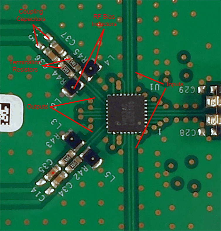
Layout for the LMH6521 is critical to achieve specified performance. Circuit symmetry is necessary for good HD2 performance. Input traces must be 200-Ω impedance transmission lines. To reduce output to input coupling, use ground plane fill between the amplifier input and output traces as shown in Figure 42. The output inductors contribute to crosstalk if placed too closely together. See Figure 42 for recommended placement of the output bias inductors. Output termination resistors and coupling capacitors must be placed as closely to the output inductors as possible.
10.2 Layout Example
 Figure 42. LMH6521 Layout Example
10.3 Thermal Considerations
The LMH6521 is packaged in a thermally enhanced WQFN package and features an exposed pad that is connected to the GND pins. TI recommends attaching the exposed pad directly to a large power supply ground plane for maximum heat dissipation. The thermal advantage of the WQFN package is fully realized only when the exposed die attach pad is soldered down to a thermal land on the PCB board with the through vias planted underneath the thermal land. The thermal land can be connected to any ground plane within the PCB. However, it is also very important to maintain good high-speed layout practices when designing a system board.
The LMH6521EVAL evaluation board implemented an eight metal layer PCB with (a) 4 oz. copper inner ground planes (b) additonal through vias and (c) maximum bottom layer metal coverage to assist with device heat dissipation. These PCB design techniques assist with the heat dissipation of the LMH6521 to optimize distortion performance. See AN–2045 LMH6521EVAL Evaluation Board (SNOA551) for suggested layout techniques.