ZHCSGX2E May 2011 – August 2016 LMH6521
PRODUCTION DATA.
- 1 特性
- 2 应用
- 3 说明
- 4 修订历史记录
- 5 Pin Configuration and Functions
- 6 Specifications
- 7 Detailed Description
- 8 Application and Implementation
- 9 Power Supply Recommendations
- 10Layout
- 11器件和文档支持
- 12机械、封装和可订购信息
7 Detailed Description
7.1 Overview
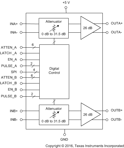
The LMH6521 is a dual, digitally controlled variable gain amplifier designed for narrowband and wideband intermediate frequency sampling applications. The LMH6521 is optimized for accurate 0.5-dB gain steps with exceptional gain and phase matching between channels combined with low distortion products. Gain matching error is less than ±0.05 dB and phase matching error less than ±0.5° over the entire attenuation range. This makes the LMH6521 ideal for driving analog-to-digital converters where high linearity is necessary. Figure 38 shows a typical application circuit.
The LMH6521 has been designed for AC-coupled applications and has been optimized to operate at frequencies greater than 3 MHz.
7.2 Functional Block Diagram
7.3 Feature Description
7.3.1 Input Characteristics
The LMH6521 input impedance is set by internal resistors to a nominal 200 Ω. At higher frequencies, device parasitic reactances starts to impact the input impedances. See Figure 21 in Typical Characteristics for more details.
For many AC-coupled applications, the impedance can be easily changed using LC circuits to transform the actual impedance to the desired impedance.
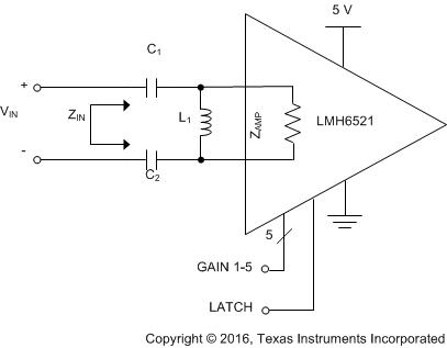 Figure 23. Differential 200-Ω LC Conversion Circuit
In Figure 23 a circuit is shown that matches the amplifier 200-Ω input with a source impedance of 100 Ω.
To avoid undesirable signal transients, the LMH6521 must not be powered on with large inputs signals present. Careful planning of system power on sequencing is especially important to avoid damage to ADC inputs.
7.3.2 Output Characteristics
The LMH6521 has a low output impedance very similar to a traditional operational amplifier output. This means that a wide range of load impedance can be driven with minimal gain loss. Matching load impedance for proper termination of filters is as easy as inserting the proper value of resistor between the filter and the amplifier. This flexibility makes system design and gain calculations very easy. The LMH6521 was designed to run from a single 5-V supply. In spite of this low supply voltage the LMH6521 is still able to deliver very high power gains when driving low impedance loads.
7.3.3 Output Connections
The LMH6521, like most high frequency amplifiers, is sensitive to loading conditions on the output. Load conditions that include small amounts of capacitance connected directly to the output can cause stability problems. An example of this is shown in Figure 24. A more sophisticated filter may require better impedance matching. See Figure 36 for an example filter configuration and table Table 7 for some IF filter components values.
 Figure 24. Example Output Configuration
The outputs of the LMH6521 must be biased near the ground potential. On the evaluation board, 1-µH inductors are installed to provide proper output biasing. The bias current is approximately 36 mA per output pin and is not a function of the load condition, which makes the LMH6521 robust to handle various output load conditions while maintaining superior linearity as shown in Figure 25. With large inductors and high operating frequencies the inductor presents a very high impedance and has minimal AC current. If the inductor is chosen to have a smaller value, or if the operating frequency is very low there could be enough AC current flowing in the inductor to become significant. Make sure to check the inductor datasheet to not exceed the maximum current limit.
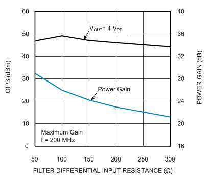 Figure 25. OIP3 vs Amplifier Load Resistance
7.4 Device Functional Modes
The LMH6521 is a differential input, differential output, digitally controlled variable gain amplifier (DVGA). This is the primary functional mode. The LMH6521 is designed to support large voltage swings with excellent linearity. For this reason the amplifier output stage is biased separately than the rest of the amplifier. Like many RF amplifiers, the LMH6521 output stage is powered through the output pins.
Power to the LMH6521 output stage is accomplished by using RF chokes to supply the DC current required by the output transistors. The EVM and all data sheet plots were derived using 1-µH RF chokes. Other values can be used if desired. The rule of thumb is that using a larger value RF choke improves low-frequency performance while using a smaller RF choke improves high-frequency performance. RF chokes must be between 10 µH and 300 nH in value. Values outside this range can work, but performance must be thoroughly verified before committing to a design.
7.5 Programming
7.5.1 Digital Control
The LMH6521 supports three modes of gain control: parallel mode, serial mode (SPI compatible), and pulse mode. Parallel mode is fastest and requires the most board space for logic line routing. Serial mode is compatible with existing SPI compatible systems. The pulse mode is both fast and compact, but must step through intermediate gain steps when making large gain changes.
Pins MOD0 and MOD1 are used to configure the LMH6521 for the three gain control modes. MOD0 and MOD1 have weak pullup resistors to an internal 2.5-V reference but is designed for 2.5-V to 5-V CMOS logic levels. MOD0 and MOD1 can be externally driven (LOGIC HIGH) to voltages between 2.5 V to 5 V to configure the LMH6521 into one of the three digital control modes. Some pins on the LMH6521 have different functions depending on the digital control mode. Table 1 lists these functions.
Table 1. Digital Control Mode Pin Functions
| PIN NUMBER | PARALLEL MODE | SERIAL MODE | PULSE MODE |
| 1 | A3 | SDI | DNA |
| 2 | A4 | CLK | UPA |
| 3 | A5 | NC | GND |
| 4 (MOD0) | LOGIC HIGH (MOD0=1) | LOGIC LOW (MOD0=0) | LOGIC HIGH (MOD0=1) |
| 5 (MOD1) | LOGIC HIGH (MOD1=1) | LOGIC HIGH (MOD1=1) | LOGIC LOW (MOD1=0) |
| 6 | B5 | GND | GND |
| 7 | B4 | NC | UPB |
| 8 | B3 | NC | DNB |
| 9 | B2 | NC | S1B |
| 10 | B1 | NC | S0B |
| 11 | INB+ | ||
| 12 | INB- | ||
| 13 | GND | ||
| 14 | +5 V | ||
| 15 | GND | ||
| 16 | B0 | GND | GND |
| 17 | OUTB+ | ||
| 18 | OUTB- | ||
| 19 | ENB | ||
| 20 | LATB | GND | GND |
| 21 | LATA | GND | GND |
| 22 | ENA | ||
| 23 | OUTA- | ||
| 24 | OUTA+ | ||
| 25 | A0 | NC | GND |
| 26 | GND | ||
| 27 | +5 V | ||
| 28 | GND | ||
| 29 | INA- | ||
| 30 | INA+ | ||
| 31 | A1 | SDO | S0A |
| 32 | A2 | CS | S1A |
7.5.2 Parallel Mode (MOD1 = 1, MOD0 = 1)
When designing a system that requires very fast gain changes parallel mode is the best selection. See Table 1 for pin definitions of the LMH6521 in parallel mode.
The LMH6521 has a 6-bit gain control bus as well as latch pins LATA and LATB for channels A and B. When the latch pin is low, data from the gain control pins is immediately sent to the gain circuit (that is, gain is changed immediately). When the latch pin transitions high the current gain state is held and subsequent changes to the gain set pins are ignored. To minimize gain change glitches multiple gain control pins must not change while the latch pin is low. Gain glitches could result from timing skew between the gain set bits. This is especially the case when a small gain change requires a change in state of three or more gain control pins. If continuous gain control is desired the latch pin can be tied to ground. This state is called transparent mode and the gain pins are always active. In this state the timing of the gain pin logic transitions must be planned carefully to avoid undesirable transients
ENA and ENB pins are provided to reduce power consumption by disabling the highest power portions of the LMH6521. The gain register preserves the last active gain setting during the disabled state. These pins float high and can be left disconnected if they won't be used. If the pins are left disconnected, a 0.01-µF capacitor to ground helps prevent external noise from coupling into these pins.
Figure 26, Figure 27, and Figure 28 show the various connections in parallel mode with respect to the latch pin.
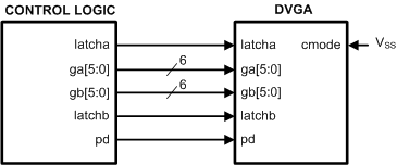 Figure 26. Parallel Mode Connection for Fastest Response
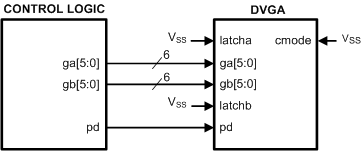
 Figure 28. Parallel Mode Connection Using Latch Pins to Mulitplex Digital Data
7.5.3 Serial Mode: SPI Compatible Interface (MOD1 = 1, MOD0 = 0)
Serial interface allows a great deal of flexibility in gain programming and reduced board complexity. Using only 4 wires for both channels allows for significant board space savings. The trade-off for this reduced board complexity is slower response time in gain state changes. For systems where gain is changed only infrequently or where only slow gain changes are required serial mode is the best choice. See Table 1 table for pin definitions of the LMH6521 in serial mode.
The serial interface is a generic 4-wire synchronous interface that is compatible with SPI standard interfaces and used on many microcontrollers and DSP controllers.
The serial mode is active when the two mode pins are set as follows: MOD1=1, MOD0=0). In this configuration the pins function as shown in Pin Configuration and Functions. The SPI interface uses the following signals: clock input (CLK), serial data in (SDI), serial data out, and serial chip select (CS)
ENA and ENB pins are active in serial mode. For fast disable capability these pins can be used and the serial register holds the last active gain state. These pins float high and can be left disconnected for serial mode. The serial control bus can also disable the DVGA channels, but at a much slower speed. The serial enable function is an AND function. For a channel to be active both the enable pin and the serial control register must be in the enabled state. To disable a channel, either method will suffice. See Typical Characteristics for disable and enable timing information.
LATA and LATB pins are not active during serial mode.
The serial clock pin CLK is used to register the input data that is presented on the SDI pin on the rising edge; and to source the output data on the SDO pin on the falling edge. User may disable clock and hold it in the low state, as long as the clock pulse-width minimum specification is not violated when the clock is enabled or disabled.
The chip select pin CS starts a new register access with each assertion; that is, the SDATA field protocol is required. The user is required to deassert this signal after the 16th clock. If the SCSb is deasserted before the 16th clock, no address or data write will occur. The rising edge captures the address just shifted-in and, in the case of a write operation, writes the addressed register. There is a minimum pulse-width requirement for the deasserted pulse - which is specified in Electrical Characteristics.
SDI is an input pin for the serial data. It must observe setup or hold requirements with respect to the SCLK. Each cycle is 16-bits long
SDO is the data output pin and is normally at TRI-STATE and is driven only when SCSb is asserted. Upon SCSb assertion, contents of the register addressed during the first byte are shifted out with the second 8 SCLK falling edges. Upon power up, the default register address is 00h.
The SDO internal driver circuit is an open-collector device with a weak pullup resistor to an internal 2.5-V reference. It is 5-V tolerant so an external pullup resistor can connect to 2.5 V, 3.3 V, or 5 V as shown in Figure 30. However, the external pullup resistor must be chosen to limit the current to 11 mA or less. Otherwise the SDO logic low output level (VOL) may not achieve close to ground and in extreme case could cause problem for FPGA input gate. Using minimum values for external pullup resistor is a good to maximize speed for SDO signal. So if high SPI clock frequency is required, then minimum value external pullup resistor is the best choice as shown in Figure 30.
Each serial interface access cycle is exactly 16 bits long as shown in Figure 29. Each signal's function is described below. The read timing is shown in Figure 31, while the write timing is shown in figure Figure 32.
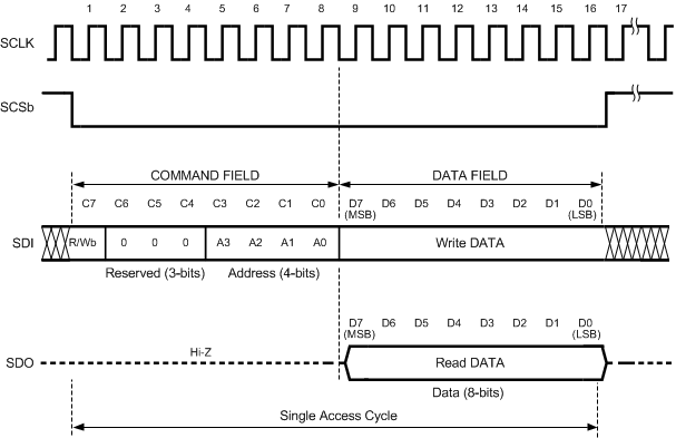 Figure 29. Serial Interface Protocol (SPI Compatible)
Table 2. Serial Interface Protocol
| ADDRESS | DESCRIPTION |
| R/Wb | Read / Write bit. A value of 1 indicates a read operation, while a value of 0 indicates a write operation. |
| Reserved | Not used. Must be set to 0. |
| ADDR | Address of register to be read or written. |
| DATA | In a write operation the value of this field is written to the addressed register when the chip select pin is deasserted. In a read operation this field is ignored. |
Table 3. Serial Word Format for LMH6521
| C7 | C6 | C5 | C4 | C3 | C2 | C1 | C0 |
| 0 = write 1 = read |
0 | 0 | 0 | 0 | 0 | 0 | 0 = Ch A 1 = Ch B |
Table 4. Serial Word Format for LMH6521 (cont)
| Enable | Gb5 | Gb4 | Gb3 | Gb2 | Gb1 | Gb0 | RES |
| 0 = Off 1 = On |
1 = +16 dB | 1 = +8 dB | 1 = +4 dB | 1 = +2 dB | 1 = +1 dB | 1 = +0.5 dB | 0 |
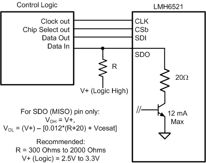 Figure 30. Serial Mode 4–Wire Connection
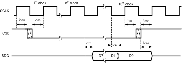 Figure 31. Read Timing
Table 5. Read Timing, Data Output on SDO Pin
| PARAMETER | DESCRIPTION |
|---|---|
| tCSH | Chip select hold time |
| tCSS | Chip select setup time |
| tOZD | Initial output data delay |
| tODZ | High impedance delay |
| tOD | Output data delay |
 Figure 32. Write Timing, Data Written to SDI Pin
Table 6. Write Timing, Data Input on SDI Pin
| PARAMETER | DESCRIPTION |
| tPL | Minimum clock low time (clock duty dycle) |
| tPH | Minimum clock high time (clock duty cycle) |
| tSU | Input data setup time |
| tH | Input data hold time |
7.5.4 Pulse Mode (MOD1 = 0, MOD0 = 1)
Pulse mode is a simple yet fast way to adjust gain settings. Using only two control lines per channel the LMH6521 gain can be changed by simple up and down signals. Gain step sizes is selectable either by hard wiring the board or using two additional logic inputs. For a system where gain changes can be stepped sequentially from one gain to the next and where board space is limited this mode may be the best choice. The ENA and ENB pins are fully active during pulse mode, and the channel gain state is preserved during the disabled state. See Table 1 for pin definitions of the LMH6521 in pulse mode.
In this mode the gain step size can be selected from a choice of 0.5-, 1-, 2-, or 6-dB steps. During operation the gain can be quickly adjusted either up or down one step at a time by a negative pulse on the UP or DN pins. As shown in Figure 34, each gain step pulse must have a logic high state of at least tPW= 20 ns and a logic low state of at least tPG= 20 ns for the pulse to register as a gain change signal.
 Figure 33. Pulse Timing
To provide a known gain state, there is a reset feature in pulse mode. To reset the gain to maximum gain both the UP and DN pins must be strobed low together as shown in Figure 34. There must be an overlap of at least tRW = 20 ns for the reset to register.
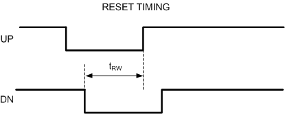 Figure 34. Pulse Mode Timing
7.5.5 Interface to ADC
The LMH6521 was designed to be used with TI's high speed ADC's. As shown in Figure 38, AC coupling provides the best flexibility especially for IF sub-sampling applications.
The inputs of the LMH6521 will self bias to the optimum voltage for normal operation. The internal bias voltage for the inputs is approximately mid-rail which is 2.5 V with the typical 5-V power supply condition. In most applications the LMH6521 input is required to be AC coupled.
The LMH6521 output common mode voltage is biased to 0 V and has a maximum differential output voltage swing of 10 VPPD as shown in Figure 35. This means that for driving most ADCs AC coupling is required. Because most often a band pass filter is desired, the amplifier and ADC the bandpass filter can be configured to block the DC voltage of the amplifier output from the ADC input. Figure 36 shows a wideband bandpass filter configuration that could be designed for a 200-Ω impedance system for various IF frequencies.
 Figure 35. Output Voltage with Respect to Output Common Mode
 Figure 36. Wideband Bandpass Filter
Table 7 shows values for some common IF frequencies for Figure 36. The filter shown in Figure 36 offers a good compromise between bandwidth, noise rejection, and cost. This filter topology works best with the 12- to 16-bit analog to digital converters shown in Table 8.
Table 7. IF Frequency Bandpass Filter Component Values
| CENTER FREQUENCY | 75 MHz | 150 MHz | 180 MHz | 250 MHz |
| Bandwidth | 40 MHz | 60 MHz | 75 MHz | 100 MHz |
| R1, R2 | 90 Ω | 90 Ω | 90 Ω | 90 Ω |
| L1, L2 | 390 nH | 370 nH | 300 nH | 225 nH |
| C1, C2 | 10 pF | 3 pF | 2.7 pF | 1.9 pF |
| C3 | 22 pF | 19 pF | 15 pF | 11 pF |
| L5 | 220 nH | 62 nH | 54 nH | 36 nH |
| R3, R4 | 100 Ω | 100 Ω | 100 Ω | 100 Ω |
Table 8. Compatible High-Speed Analog-to-Digital Converters
| PRODUCT NUMBER | MAX SAMPLING RATE (MSPS) | RESOLUTION | CHANNELS |
|---|---|---|---|
| ADC12L063 | 62 | 12 | SINGLE |
| ADC12DL065 | 65 | 12 | DUAL |
| ADC12L066 | 66 | 12 | SINGLE |
| ADC12DL066 | 66 | 12 | DUAL |
| CLC5957 | 70 | 12 | SINGLE |
| ADC12L080 | 80 | 12 | SINGLE |
| ADC12DL080 | 80 | 12 | DUAL |
| ADC12C080 | 80 | 12 | SINGLE |
| ADC12C105 | 105 | 12 | SINGLE |
| ADC12C170 | 170 | 12 | SINGLE |
| ADC12V170 | 170 | 12 | SINGLE |
| ADC14C080 | 80 | 14 | SINGLE |
| ADC14C105 | 105 | 14 | SINGLE |
| ADC14DS105 | 105 | 14 | DUAL |
| ADC14155 | 155 | 14 | SINGLE |
| ADC14V155 | 155 | 14 | SINGLE |
| ADC16V130 | 130 | 16 | SINGLE |
| ADC16DV160 | 160 | 16 | DUAL |
| ADC08D500 | 500 | 8 | DUAL |
| ADC08500 | 500 | 8 | SINGLE |
| ADC08D1000 | 1000 | 8 | DUAL |
| ADC081000 | 1000 | 8 | SINGLE |
| ADC08D1500 | 1500 | 8 | DUAL |
| ADC081500 | 1500 | 8 | SINGLE |
| ADC08(B)3000 | 3000 | 8 | SINGLE |
| ADC08L060 | 60 | 8 | SINGLE |
| ADC08060 | 60 | 8 | SINGLE |
| ADC10DL065 | 65 | 10 | DUAL |
| ADC10065 | 65 | 10 | SINGLE |
| ADC10080 | 80 | 10 | SINGLE |
| ADC08100 | 100 | 8 | SINGLE |
| ADCS9888 | 170 | 8 | SINGLE |
| ADC08(B)200 | 200 | 8 | SINGLE |
| ADC11C125 | 125 | 11 | SINGLE |
| ADC11C170 | 170 | 11 | SINGLE |
An alternate narrowband filter approach is presented in Figure 37. The narrow band-pass antialiasing filter between the LMH6521 and ADC16DV160 attenuates the output noise of the LMH6521 outside the Nyquist zone helping to preserve the available SNR of the ADC. Figure 37 shows a 1:4 input transformer used to match the 200-Ω balanced input of the LMH6521 to the 50 unbalanced source to minimize insertion lost at the input. Figure 37 shows the LMH6521 driving the ADC16DV160 (16-bit ADC). The band-pass filter is a 3rd order 100-Ω matched tapped-L configured for a center frequency of 192 MHz with a 20-MHz bandwidth across the differential inputs of the ADC16DV160. The ADC16DV160 is a dual channel 16-bit ADC with maximum sampling rate of
160 MSPS. Using a 2-tone large input signal with the LMH6521 set to maximum gain (26dB) to drive an input signal level at the ADC of –1 dBFS, the SNR and SFDR results are shown in Table 9.

Table 9. LMH6521+BPF+ADC16DV160 vs Typical ADC16DV160 Specifications
| CONFIGURATION | ADC INPUT | SNR (dBFS) | SFDR (dBFS) |
|---|---|---|---|
| LMH6521+BPF+ADC16DV160 | –1 dBFS | 75.5 | 82 |
| ADC16DV160 only | –1 dBFS | 76 | 89 |