SNOSAK7D February 2005 – January 2015 LMH6551
PRODUCTION DATA.
- 1 Features
- 2 Applications
- 3 Description
- 4 Typical Application
- 5 Revision History
- 6 Pin Configuration and Functions
- 7 Specifications
- 8 Detailed Description
- 9 Application and Implementation
- 10Power Supply Recommendations
- 11Layout
- 12Device and Documentation Support
- 13Mechanical, Packaging, and Orderable Information
8 Detailed Description
8.1 Overview
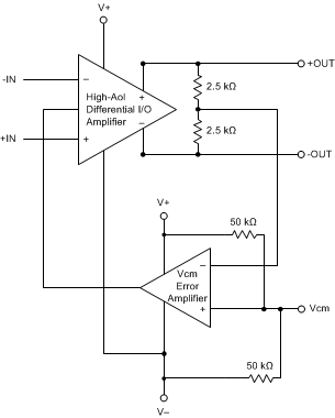
The LMH6551 is a fully differential amplifier designed to provide low distortion amplification to wide bandwidth differential signals. The LMH6551, though fully integrated for ultimate balance and distortion performance, functionally provides three channels. Two of these channels are the V+ and V− signal path channels, which function similarly to inverting mode operational amplifiers and are the primary signal paths. The third channel is the common-mode feedback circuit. This is the circuit that sets the output common mode as well as driving the V+ and V− outputs to be equal magnitude and opposite phase, even when only one of the two input channels is driven. The common-mode feedback circuit allows single-ended to differential operation.
8.2 Functional Block Diagram

8.3 Feature Description
The LMH6551 combines a core differential I/O, high-gain block with an output common-mode sense that is compared to a reference voltage and then fed back into the main amplifier block to control the average output to that reference. The differential I/O block is a classic, high open-loop gain stage. The high-speed differential outputs include an internal averaging resistor network to sense the output common-mode voltage. This voltage is compared by a separate VCM error amplifier to the voltage on the VOCM pin. If floated, this reference is at half the total supply voltage across the device using two 50-kΩ resistors. This VCM error amplifier transmits a correction signal into the main amplifier to force the output average voltage to meet the target voltage on the VOCM pin.
8.4 Device Functional Modes
This wideband FDA requires external resistors for correct signal-path operation. When configured for the desired input impedance and gain setting with these external resistors, the amplifier can be either on with the PD pin asserted to a voltage greater than Vs– + 1.7 V, or turned off by asserting PD low. Disabling the amplifier shuts off the quiescent current and stops correct amplifier operation. The signal path is still present for the source signal through the external resistors. The VOCM control pin sets the output average voltage. Left open, VOCM defaults to an internal midsupply value. Driving this high-impedance input with a voltage reference within its valid range sets a target for the internal VCM error amplifier.