SNOSAK9F June 2006 – June 2015 LMH6601 , LMH6601-Q1
PRODUCTION DATA.
- 1 Features
- 2 Applications
- 3 Description
- 4 Revision History
- 5 Pin Configuration and Functions
-
6 Specifications
- 6.1 Absolute Maximum Ratings
- 6.2 ESD Ratings - for LMH6601
- 6.3 ESD Ratings - for LMH6601-Q1
- 6.4 Recommended Operating Conditions
- 6.5 Thermal Information
- 6.6 Electrical Characteristics, 5 V
- 6.7 Electrical Characteristics, 3.3 V
- 6.8 Electrical Characteristics, 2.7 V
- 6.9 Switching Characteristics, 5 V
- 6.10 Switching Characteristics, 3.3 V
- 6.11 Switching Characteristics, 2.7 V
- 6.12 Typical Characteristics
- 7 Detailed Description
- 8 Application and Implementation
- 9 Power Supply Recommendations
- 10Layout
- 11Device and Documentation Support
- 12Mechanical, Packaging, and Orderable Information
8 Application and Implementation
NOTE
Information in the following applications sections is not part of the TI component specification, and TI does not warrant its accuracy or completeness. TI’s customers are responsible for determining suitability of components for their purposes. Customers should validate and test their design implementation to confirm system functionality.
8.1 Application Information
8.1.1 DC-Coupled, Single-Supply Baseband Video Amplifier and Driver
The LMH6601 output can swing very close to either rail to maximize the output dynamic range which is of particular interest when operating in a low-voltage, single-supply environment. Under light output load conditions, the output can swing as close as a few mV of either rail. This also allows a video amplifier to preserve the video black level for excellent video integrity. In the example shown in Figure 51, the baseband video output is amplified and buffered by the LMH6601 which then drives the 75-Ω back-terminated video cable for an overall gain of +1 delivered to the 75-Ω load. The input video would normally have a level between 0 V to approximately 0.75 V.
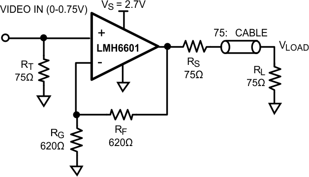 Figure 51. Single-Supply Video Driver Capable of Maintaining Accurate Video Black Level
With the LMH6601 input common-mode range including the V− (ground) rail, there will be no need for AC-coupling or level shifting and the input can directly drive the noninverting input which has the additional advantage of high amplifier input impedance. With LMH6601’s wide rail-to-rail output swing, as stated earlier, the video black level of 0 V is maintained at the load with minimal circuit complexity and using no AC-coupling capacitors. Without true rail-to-rail output swing of the LMH6601, and more importantly without the LMH6601’s ability of exceedingly close swing to V−, the circuit would not operate properly as shown at the expense of more complexity. This circuit will also work for higher input voltages. The only significant requirement is that there is at least 1.8 V from the maximum input voltage to the positive supply (V+).
The Composite Video Output of some low-cost consumer video equipment consists of a current source which develops the video waveform across a load resistor (usually 75 Ω), as shown in Figure 52. With these applications, the same circuit configuration just described and shown in Figure 52 will be able to buffer and drive the Composite Video waveform which includes sync and video combined. However, with this arrangement, the LMH6601 supply voltage must be at least 3.3 V or higher to allow proper input common-mode voltage headroom because the input can be as high as 1-V peak.
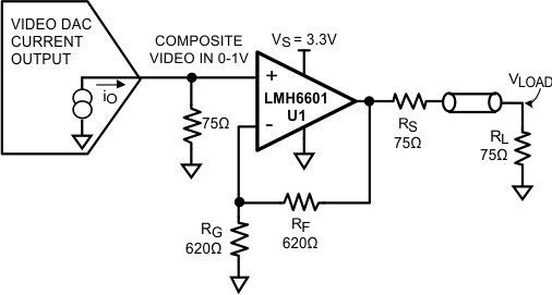 Figure 52. Single-Supply Composite Video Driver for Consumer Video Outputs
If the Video In signal is Composite Video with negative going Sync tip, a variation of the previous configurations should be used. This circuit produces a unipolar (more than 0 V) DC-coupled single-supply video signal as shown in Figure 53.
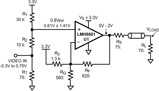 Figure 53. Single-Supply, DC-Coupled Composite Video Driver for Negative Going Sync Tip
In the circuit of Figure 53, the input is shifted positive by means of R1, R2, and RT in order to satisfy the common-mode input range of the U1. The signal will loose 20% of its amplitude in the process. The closed-loop gain of U1 must be set to make up for this 20% loss in amplitude. This gives rise to the gain expression shown in Equation 1, which is based on a getting a 2 VPP output with a 0.8 VPP input:

R3 will produce a negative shift at the output due to VS (3.3 V in this case). R3 must be set so that the Video In sync tip (−0.3 V at RT or 0.61 V at U1 noninverting input) corresponds to near 0 V at the output.

Equation 1 and Equation 2 must be solved simultaneously to arrive at the values of R3, RF, and RG which will satisfy both. From the data sheet, one can set RF = 620 Ω to be close to the recommended value for a gain of +2. It is easier to solve for RG and R3 by starting with a good estimate for one and iteratively solving Equation 1 and Equation 2 to arrive at the results. Here is one possible iteration cycle for reference:
Table 1. Finding External Resistor Values by Iteration for Figure 53
| ESTIMATE RG (Ω) |
CALCULATED (from Equation 2) R3 (Ω) |
Equation 1 LHS CALCULATED |
COMMENT (COMPARE Equation 1 LHS calculated to RHS) |
|---|---|---|---|
| 1k | 1.69k | 0.988 | Increase Equation 1 LHS by reducing RG |
| 820 | 1.56k | 1.15 | Increase Equation 1 LHS by reducing RG |
| 620 | 1.37k | 1.45 | Increase Equation 1 LHS by reducing RG |
| 390 | 239 | 4.18 | Reduce Equation 1 LHS by increasing RG |
| 560 | 1.30k | 1.59 | Close to target value of 1.5V/V for Equation 1 |
The final set of values for RG and R3 in Table 1 are values which will result in the proper gain and correct video levels (0 V to 1 V) at the output (VLOAD).
8.1.2 How to Pick the Right Video Amplifier
Apart from output current drive and voltage swing, the op amp used for a video amplifier and cable driver should also possess the minimum requirement for speed and slew rate. For video type loads, it is best to consider Large Signal Bandwidth (or LSBW in the TI data sheet tables) as video signals could be as large as 2 VPP when applied to the commonly used gain of +2 configuration. Because of this relatively large swing, the op amp Slew Rate (SR) limitation should also be considered. Table 2 shows these requirements for various video line rates calculated using a rudimentary technique and intended as a first-order estimate only.
Table 2. Rise Time, −3 dB BW, and Slew Rate Requirements for Various Video Line Rates
| VIDEO STANDARD |
LINE RATE (HxV) |
REFRESH RATE (Hz) |
HORIZONTAL ACTIVE (KH%) |
VERTICAL ACTIVE (KV%) |
PIXEL TIME (ns) |
RISE TIME (ns) |
LSBW (MHz) |
SR (V/μs) |
|---|---|---|---|---|---|---|---|---|
| TV_NTSC | 451x483 | 30 | 84 | 92 | 118.3 | 39.4 | 9 | 41 |
| VGA | 640x480 | 75 | 80 | 95 | 33 | 11 | 32 | 146 |
| SVGA | 800x600 | 75 | 76 | 96 | 20.3 | 6.8 | 52 | 237 |
| XGA | 1024x768 | 75 | 77 | 95 | 12.4 | 4.1 | 85 | 387 |
| SXGA | 1280x1024 | 75 | 75 | 96 | 7.3 | 2.4 | 143 | 655 |
| UXGA | 1600x1200 | 75 | 74 | 96 | 4.9 | 1.6 | 213 | 973 |
For any video line rate (HxV corresponding to the number of Active horizontal and vertical lines), the speed requirements can be estimated if the Horizontal Active (KH%) and Vertical Active (KV%) numbers are known. These percentages correspond to the percentages of the active number of lines (horizontal or vertical) to the total number of lines as set by VESA standards. Here are the general expressions and the specific calculations for the SVGA line rate shown in Table 2.
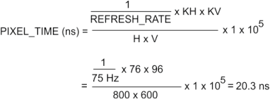
Requiring that an “On” pixel is illuminated to at least 90 percent of its final value before changing state will result in the rise/fall time equal to, at most, ⅓ the pixel time as shown in Equation 5:

Assuming a single pole frequency response roll-off characteristic for the closed-loop amplifier used, we have:

Rise/Fall times are 10%-90% transition times, which for a 2 VPP video step would correspond to a total voltage shift of 1.6V (80% of 2 V). So, the Slew Rate requirement can be calculated as follows:

The LMH6601 specifications show that it would be a suitable choice for video amplifiers up to and including the SVGA line rate as demonstrated above.
For more information about this topic and others relating to video amplifiers, see Application Note 1013, Video Amplifier Design for Computer Monitors (SNVA031).
8.1.3 Current to Voltage Conversion (Transimpedance Amplifier (TIA)
Being capable of high speed and having ultra low input bias current makes the LMH6601 a natural choice for Current to Voltage applications such as photodiode I-V conversion. In these type of applications, as shown in Figure 54, the photodiode is tied to the inverting input of the amplifier with RF set to the proper gain (gain is measured in Ω).
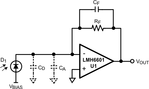 Figure 54. Typical Connection of a Photodiode Detector to an Op Amp
With the LMH6601 input bias current in the femto-amperes range, even large values of gain (RF) do not increase the output error term appreciably. This allows circuit operation to a lower light intensity level which is always of special importance in these applications. Most photo-diodes have a relatively large capacitance (CD) which would be even larger for a photo-diode designed for higher sensitivity to light because of its larger area. Some applications may run the photodiode with a reverse bias to reduce its capacitance with the disadvantage of increased contributions from both dark current and noise current. Figure 55 shows a typical photodiode capacitance plot vs. reverse bias for reference.
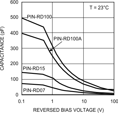 Figure 55. Typical Capacitance vs. Reverse Bias (Source: OSI Optoelectronics)
The diode capacitance (CD) combined with the input capacitance of the LMH6601 (CA) has a bearing on the stability of this circuit and how it is compensated. With large transimpedance gain values (RF), the total combined capacitance on the amplifier inverting input (CIN = CD + CA) will work against RF to create a zero in the Noise Gain (NG) function (see Figure 56). If left untreated, at higher frequencies where NG equals the open-loop transfer function excess phase shift around the loop (approaching 180°) and therefore, the circuit could be unstable. This is illustrated in Figure 56.
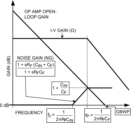 Figure 56. Transimpedance Amplifier Graphical Stability Analysis and Compensation
Figure 56 shows that placing a capacitor, CF, with the proper value, across RF will create a pole in the NG function at fP. For optimum performance, this capacitor is usually picked so that NG is equal to the open-loop gain of the op amp at fP. This will cause a “flattening” of the NG slope beyond the point of intercept of the two plots (open-loop gain and NG) and will results in a Phase Margin (PM) of 45° assuming fP and fZ are at least a decade apart. This is because at the point of intercept, the NG pole at fP will have a 45° phase lead contribution which leaves 45° of PM. For reference, Figure 56 also shows the transimpedance gain (I-V (Ω))
Here is the theoretical expression for the optimum CF value and the expected −3-dB bandwidth:


Table 3 lists the results, along with the assumptions and conditions, of testing the LMH6601 with various photodiodes having different capacitances (CD) at a transimpedance gain (RF) of 10 kΩ.
Table 3. Transimpedance Amplifier Compensation and Performance Results for Figure 54
| CD
(pF) |
CIN
(pF) |
CF_CALCULATED (pF) |
CF USED (pF) |
−3 dB BW CALCULATED (MHz) |
−3 dB BW MEASURED (MHz) |
STEP RESPONSE OVERSHOOT (%) |
|---|---|---|---|---|---|---|
| 10 | 12 | 1.1 | 1 | 14 | 15 | 6 |
| 50 | 52 | 2.3 | 3 | 7 | 7 | 4 |
| 500 | 502 | 7.2 | 8 | 2 | 2.5 | 9 |
8.1.4 Transimpedance Amplifier Noise Considerations
When analyzing the noise at the output of the I-V converter, it is important to note that the various noise sources (that is, op amp noise voltage, feedback resistor thermal noise, input noise current, photodiode noise current) do not all operate over the same frequency band. Therefore, when the noise at the output is calculated, this should be taken into account.
The op amp noise voltage will be gained up in the region between the noise gain’s “zero” and its “pole” (fz and fp in Figure 56). The higher the values of RF and CIN, the sooner the noise gain peaking starts and therefore its contribution to the total output noise would be larger. It is obvious to note that it is advantageous to minimize CIN (for example, by proper choice of op amp, by applying a reverse bias across the diode at the expense of excess dark current and noise). However, most low noise op amps have a higher input capacitance compared to ordinary op amps. This is due to the low noise op amp’s larger input stage.
8.1.5 Charge Preamplifier
 Figure 57. Charge Preamplifier Taking Advantage of the Femto-Ampere Range Input Bias Current of the LMH6601
8.1.6 Capacitive Load
The LMH6601 can drive a capacitive load of up to 1000 pF with correct isolation and compensation. Figure 58 illustrates the in-loop compensation technique to drive a large capacitive load.
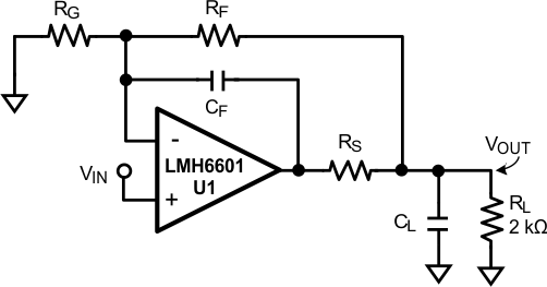 Figure 58. In-Loop Compensation Circuit for Driving a Heavy Capacitive Load
When driving a high-capacitive load, an isolation resistor (RS) should be connected in series between the op amp output and the capacitive load to provide isolation and to avoid oscillations. A small-value capacitor (CF) is inserted between the op amp output and the inverting input as shown such that this capacitor becomes the dominant feedback path at higher frequency. Together these components allow heavy capacitive loading while keeping the loop stable.
There are few factors which affect the driving capability of the op amp:
- Op amp internal architecture
- Closed-loop gain and output capacitor loading
Table 4 shows the measured step response for various values of load capacitors (CL), series resistor (RS) and feedback resistor (CF) with gain of +2 (RF = RG = 604 Ω) and RL = 2 kΩ:
Table 4. LMH6601 Step Response Summary for the Circuit of Figure 58
| CL
(pF) |
RS
(Ω) |
CF
(pF) |
trise/ tfall
(ns) |
OVERSHOOT (%) |
|---|---|---|---|---|
| 10 | 0 | 1 | 6(1) | 8 |
| 50 | 0 | 1 | 7(1) | 6 |
| 110 | 47 | 1 | 10 | 16 |
| 300 | 6 | 10 | 12 | 20 |
| 500 | 80 | 10 | 33 | 10 |
| 910 | 192 | 10 | 65 | 10 |
Figure 59 shows the increase in rise/fall time (bandwidth decrease) at VOUT with larger capacitive loads, illustrating the trade-off between the two:
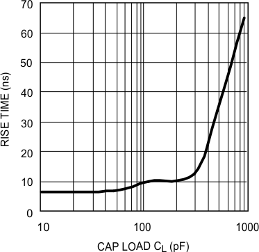 Figure 59. LMH6601 In-Loop Compensation Response
8.2 Typical Application
8.2.1 SAG Compensation for AC-Coupled Video
Many monitors and displays accept AC-coupled inputs. This simplifies the amplification and buffering task in some respects. The capacitors shown in Figure 60 (except CG2), and especially CO, are the large electrolytic type which are considerably costly and take up valuable real estate on the board. It is possible to reduce the value of the output coupling capacitor, CO, which is the largest of all, by using what is called SAG compensation. SAG refers to what the output video experiences due to the low frequency video content it contains which cannot adequately go through the output AC-coupling scheme due to the low frequency limit of this circuit. The −3 dB low frequency limit of the output circuit is given by:
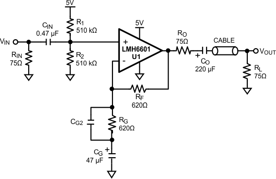 Figure 60. AC-Coupled Video Amplifier and Driver
8.2.2 Design Requirements
As shown in Figure 60, R1 and R2 simply set the input to the center of the input linear range while CIN AC couples the video onto the input of the op amp. The op amp is set for a closed-loop gain of 2 with RF and RG. CG is there to make sure the device output is also biased at mid-supply. Because of the DC bias at the output, the load must be AC-coupled as well through CO. Some applications implement a small valued ceramic capacitor (not shown) in parallel with CO which is electrolytic. The reason for this is that the ceramic capacitor will tend to shunt the inductive behavior of the Electrolytic capacitor at higher frequencies for an improved overall low impedance output.
CG2 is intended to boost the high-frequency gain to improve the video frequency response. This value is to be set and trimmed on the board to meet the specific system requirements of the application.
A possible implementation of the SAG compensation is shown in Figure 61.
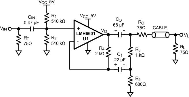 Figure 61. AC-Coupled Video Amplifier/Driver With SAG Compensation
8.2.3 Detailed Design Procedure
In the circuit of Figure 61, the output coupling capacitor value and size is reduced at the expense of a slightly more complicated circuitry. Note that C1 is not only part of the SAG compensation, but it also sets the amplifier’s DC gain to 0 dB so that the output is set to mid-rail for linearity purposes. Also, exceptionally high values are chosen for the R1 and R2 biasing resistors (510 kΩ). The LMH6601 has extremely low input bias current which allows this selection thereby reducing the CIN value in this circuit such that CIN can even be a nonpolar capacitor which will reduce cost.
At high enough frequencies where both CO and C1 can be considered to be shorted out, R3 shunts R4 and the closed-loop gain is determined by:
At intermediate frequencies, where the CO, RO, RL path experiences low frequency gain loss, the R3, R5, C1 path provides feedback from the load side of CO. With the load side gain reduced at these lower frequencies, the feedback to the op amp inverting node reduces, causing an increase at the output of the op amp as a response.
For NTSC video, low values of CO influence how much video black level shift occurs during the vertical blanking interval (∼1.5 ms) which has no video activity and thus is sensitive to the charge dissipation of the CO through the load which could cause output SAG. An especially tough pattern is the NTSC pattern called “Pulse & Bar.” With this pattern the entire top and bottom portion of the field is black level video where, for about 11 ms, CO is discharging through the load with no video activity to replenish that charge.
8.2.4 Application Curves
Figure 62 shows the output of the Figure 61 circuit highlighting the SAG.
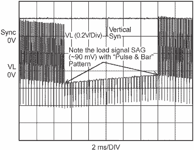 Figure 62. AC-Coupled Video Amplifier/Driver Output Scope Photo Showing Video SAG
With the circuit of Figure 61 and any other AC-coupled pulse amplifier, the waveform duty cycle variations exert additional restrictions on voltage swing at any node. This is illustrated in the waveforms shown in Figure 63.
If a stage has a 3 VPP unclipped swing capability available at a given node, as shown in Figure 63, the maximum allowable amplitude for an arbitrary waveform is ½ of 3 V or 1.5 VPP. This is due to the shift in the average value of the waveform as the duty cycle varies. Figure 63 shows what would happen if a 2 VPP signal were applied. A low duty cycle waveform, such as the one in Figure 63B, would have high positive excursions. At low enough duty cycles, the waveform could get clipped on the top, as shown, or a more subtle loss of linearity could occur prior to full-blown clipping. The converse of this occurs with high duty cycle waveforms and negative clipping, as depicted in Figure 63C.
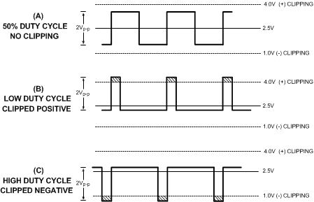 Figure 63. Headroom Considerations With AC-Coupled Amplifiers