SNOSA35G August 2002 – July 2015 LMH6657 , LMH6658
PRODUCTION DATA.
8 Application and Implementation
NOTE
Information in the following applications sections is not part of the TI component specification, and TI does not warrant its accuracy or completeness. TI’s customers are responsible for determining suitability of components for their purposes. Customers should validate and test their design implementation to confirm system functionality.
8.1 Application Information
8.1.1 Output Characteristics
8.1.1.1 Output Current Capability
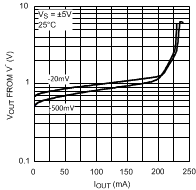
The LMH6657/6658 output swing for a given load can be determined by referring to the Output Voltage vs. Output Current plots in Typical Characteristics. Characteristic Tables show the output current when the output is 1V from either rail. The plots and table values can be used to predict closed loop continuous value of current for a given load. If left unchecked, the output current capability of the LMH6657 and LMH6658 could easily result in junction temperature exceeding the maximum allowed value specified under Absolute Maximum Ratings. Proper heat sinking or other precautions are required if conditions as such exist.
Under transient conditions, such as when the input voltage makes a large transition and the output has not had time to reach its final value, the device can deliver output currents in excess of the typical plots mentioned above. Plots shown in Figure 51 and Figure 52 depict how the output current capability improves under higher input overdrive voltages:
 Figure 51. VOUT vs. ISOURCE (for Various Overdrive)
 Figure 52. VOUT vs. ISINK (for Various Overdrive)
The LMH6657 and LMH6658 output stage is designed to swing within approximately one diode drop of each supply voltage by utilizing specially designed high speed output clamps. This allows adequate output voltage swing even with 5-V supplies and yet avoids some of the issues associated with rail-to-rail output operational amplifiers. Some of these issues are:
- Supply current increases when output reaches saturation at or near the supply rails
- Prolonged recovery when output approaches the rails
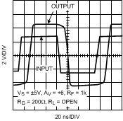
The LMH6657 and LMH6658 output is exceedingly well-behaved when it comes to recovering from an overload condition. As can be seen from Figure 53, the LMH6657 and LMH6658 will typically recover from an output overload condition in about 18 ns, regardless of the duration of the overload.
 Figure 53. Output Overload Recovery
8.1.1.2 Driving Capacitive Loads
The LMH6657 and LMH6658 can drive moderate values of capacitance by utilizing a series isolation resistor between the output and the capacitive load. Typical Characteristics shows the settling time behavior for various capacitive loads and 20 Ω of isolation resistance. Capacitive load tolerance will improve with higher closed loop gain values. Applications such as ADC buffers, among others, present complex and varying capacitive loads to the operational amplifier; best value for this isolation resistance is often found by experimentation and actual trial and error for each application.
8.1.1.3 Distortion
Applications with demanding distortion performance requirements are best served with the device operating in the inverting mode. The reason for this is that in the inverting configuration, the input common-mode voltage does not vary with the signal and there is no subsequent ill effects due to this shift in operating point and the possibility of additional non-linearity. Moreover, under low closed loop gain settings (most suited to low distortion), the noninverting configuration is at a further disadvantage of having to contend with the input common voltage range. There is also a strong relationship between output loading and distortion performance (that is, 1 kΩ vs. 100 Ω distortion improves by about 20 dB at 100 KHz) especially at the lower frequency end where the distortion tends to be lower. At higher frequency, this dependence diminishes greatly such that this difference is only about 4 dB at 10 MHz. But, in general, lighter output load leads to reduced HD3 term and thus improves THD.