SNOSD58 June 2017 LMH6702-MIL
PRODUCTION DATA.
8 Application and Implementation
NOTE
Information in the following applications sections is not part of the TI component specification, and TI does not warrant its accuracy or completeness. TI’s customers are responsible for determining suitability of components for their purposes. Customers should validate and test their design implementation to confirm system functionality.
8.1 Application Information
The LMH6702-MIL achieves its excellent pulse and distortion performance by using the current feedback topology. The loop gain for a current feedback op amp, and hence the frequency response, is predominantly set by the feedback resistor value. The LMH6702-MIL is optimized for use with a 237-Ω feedback resistor. Using lower values can lead to excessive ringing in the pulse response while a higher value will limit the bandwidth.
8.2 Typical Application
8.2.1 Feedback Resistor
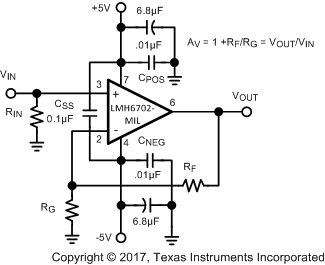
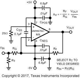
The LMH6702-MIL achieves its excellent pulse and distortion performance by using the current feedback topology. The loop gain for a current feedback op amp, and hence the frequency response, is predominantly set by the feedback resistor value. The LMH6702-MIL is optimized for use with a 237-Ω feedback resistor. Using lower values can lead to excessive ringing in the pulse response while a higher value will limit the bandwidth.
 Figure 24. Recommended Non-Inverting Gain Circuit
 Figure 25. Recommended Inverting Gain Circuit
8.2.2 Design Requirements
The exceptional performance and uniquely targeted superior technical specifications of the LMH6702-MIL make it a natural choice for high speed data acquisition applications as a front end amplifier driving the input of a high performance ADC. Of these specifications, the following can be discussed in more detail:
- A bandwidth of 1.7 GHz and relative insensitivity of bandwidth to closed loop gain (characteristic of Current Feedback architecture when compared to the traditional voltage feedback architecture) as shown in Figure 1.
- Ultra-low distortion approaching -87 dBc at the lower frequencies and exceptional noise performance (see Figure 9 and Figure 17).
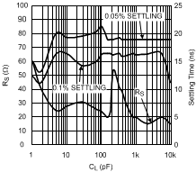
- Fast settling in less than 20 ns (see Figure 27).
As the input of an ADC could be capacitive in nature and could also alternate in capacitance value during a typical acquisition cycle, the driver amplifier (LMH6702-MIL in this case) should be designed so that it avoids instability, peaking, or other undesirable artifacts.
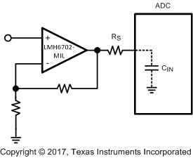
For Capacitive Load Drive, see Figure 26, which shows a typical application using the LMH6702-MIL to drive an ADC.
 Figure 26. Input Amplifier to ADC
8.2.3 Detailed Design Procedure
The series resistor, RS, between the amplifier output and the ADC input is critical to achieving best system performance. This load capacitance, if applied directly to the output pin, can quickly lead to unacceptable levels of ringing in the pulse response. Figure 27 in Application Curve (RS and Settling Time vs CL) is an excellent starting point for selecting RS. The value derived in that plot minimizes the step settling time into a fixed discrete capacitive load with the output driving a very light resistive load (1 kΩ). Sensitivity to capacitive loading is greatly reduced once the output is loaded more heavily. Therefore, for cases where the output is heavily loaded, RS value may be reduced. The exact value may best be determined experimentally for these cases.
In applications where the LMH6702-MIL is replacing the CLC409, care must be taken when the device is lightly loaded and some capacitance is present at the output. Due to the much higher frequency response of the LMH6702-MIL compared to the CLC409, there could be increased susceptibility to low value output capacitance (parasitic or inherent to the board layout or otherwise being part of the output load). As already mentioned, this susceptibility is most noticeable when the LMH6702-MIL's resistive load is light. Parasitic capacitance can be minimized by careful lay out. Addition of an output snubber R-C network will also help by increasing the high frequency resistive loading.
Referring back to Figure 26, it must be noted that several additional constraints should be considered in driving the capacitive input of an ADC. There is an option to increase RS, band-limiting at the ADC input for either noise or Nyquist band-limiting purposes. However, increasing RS too much can induce an unacceptably large input glitch due to switching transients coupling through from the convert signal. Also, CIN is oftentimes a voltage dependent capacitance. This input impedance non-linearity will induce distortion terms that will increase as RS is increased. Only slight adjustments up or down from the recommended RS value should therefore be attempted in optimizing system performance.
8.2.4 Application Curve

| AV = -1 | RL = 1 kΩ | |