SNOSD58 June   2017 LMH6702-MIL

PRODUCTION DATA.  

  1. Features
  2. Applications
  3. Description
  4. Revision History
  5. Pin Configuration and Functions
  6. Specifications
    1. 6.1 Absolute Maximum Ratings
    2. 6.2 ESD Ratings
    3. 6.3 Recommended Operating Conditions
    4. 6.4 Thermal Information
    5. 6.5 Electrical Characteristics
    6. 6.6 Typical Characteristics
  7. Detailed Description
    1. 7.1 Overview
    2. 7.2 Feature Description
      1. 7.2.1 Harmonic Distortion
    3. 7.3 Device Functional Modes
      1. 7.3.1 2-Tone 3rd Order Intermodulation
      2. 7.3.2 DC Accuracy and Noise
  8. Application and Implementation
    1. 8.1 Application Information
    2. 8.2 Typical Application
      1. 8.2.1 Feedback Resistor
      2. 8.2.2 Design Requirements
      3. 8.2.3 Detailed Design Procedure
      4. 8.2.4 Application Curve
  9. Power Supply Recommendations
  10. 10Layout
    1. 10.1 Layout Guidelines
    2. 10.2 Layout Example
  11. 11Device and Documentation Support
    1. 11.1 Documentation Support
      1. 11.1.1 Related Documentation
    2. 11.2 Community Resources
    3. 11.3 Trademarks
    4. 11.4 Electrostatic Discharge Caution
    5. 11.5 Glossary
  12. 12Mechanical, Packaging, and Orderable Information

封装选项

机械数据 (封装 | 引脚)
  • Y|0
散热焊盘机械数据 (封装 | 引脚)
订购信息

Pin Configuration and Functions

DBV Package
5-Pin SOT-23
Top View
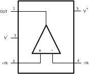
LMH6702-MIL 20039025.gif
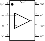
D Package
8-Pin SOIC
Top View
LMH6702-MIL 20039024.gif
NC: No internal connection

Pin Functions

PIN I/O DESCRIPTION
NAME NUMBER
D DBV
-IN 2 4 I Inverting input voltage
+IN 3 3 I Non-inverting input voltage
N/C 1, 5, 8 No connection
OUT 6 1 O Output
V- 4 2 I Negative supply
V+ 7 5 I Positive supply