ZHCSW86F July 2005 – August 2024 LMH6702QML-SP
PRODUCTION DATA
6.1.2 Harmonic Distortion
The LMH6702 has been optimized for exceptionally low harmonic distortion while driving very demanding resistive or capacitive loads. Generally, when used as the input amplifier to very high-speed flash ADCs, the distortions introduced by the converter dominate over the low LMH6702 distortions. Capacitor CSS, shown across the supplies in Figure 6-1 and Figure 6-2, is critical to achieving the lowest 2nd harmonic distortion. For absolute minimum distortion levels, keep the supply decoupling currents (ground connections to CPOS, and CNEG in Figure 6-1 and Figure 6-2) separate from the ground connections to sensitive input circuitry (such as RG, RT, and RIN ground connections). Splitting the ground plane in this manner, and separately routing the high frequency current spikes on the decoupling caps back to the power supply (similar to a star connection layout technique) provides minimum coupling back to the input circuitry and results in best harmonic distortion response (especially 2nd-order distortion).
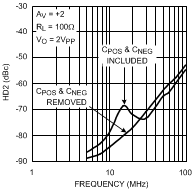
If this layout technique has not been observed on a particular application board, the supply decoupling capacitors can adversely affect HD2 performance by increasing the coupling phenomenon already mentioned. Figure 6-3 shows actual HD2 data on a board where the ground plane is shared between the supply decoupling capacitors and the rest of the circuit. After these capacitors are removed, the HD2 distortion levels reduce significantly, especially between 10MHz to 20MHz, as shown in Figure 6-3.
 Figure 6-3 Decoupling Current Adverse Effect on a Board
With Shared Ground Plane
Figure 6-3 Decoupling Current Adverse Effect on a Board
With Shared Ground PlaneAt these extremely low distortion levels, the high-frequency behavior of decoupling capacitors themselves can be significant. In general, lower-value decoupling capacitors tend to have higher resonance frequencies, making lower-value decoupling capacitors more effective for higher-frequency regions. A particular application board that has been laid out correctly with ground returns split to minimize coupling benefits the most by having low-value and higher-value capacitors paralleled to take advantage of the effective bandwidth of each, and extend the low-distortion frequency range.