SNOSAF2E February 2005 – May 2016 LMH6703
PRODUCTION DATA.
- 1 Features
- 2 Applications
- 3 Description
- 4 Revision History
- 5 Pin Configuration and Functions
- 6 Specifications
- 7 Typical Characteristics
- 8 Detailed Description
- 9 Application and Implementation
- 10Power Supply Recommendations
- 11Layout
- 12Device and Documentation Support
- 13Mechanical, Packaging, and Orderable Information
9 Application and Implementation
NOTE
Information in the following applications sections is not part of the TI component specification, and TI does not warrant its accuracy or completeness. TI’s customers are responsible for determining suitability of components for their purposes. Customers should validate and test their design implementation to confirm system functionality.
9.1 Typical Application
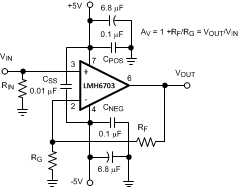
 Figure 29. Recommended Non-Inverting Gain Circuit
(SOIC Pinout Shown)
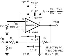
 Figure 30. Recommended Inverting Gain Circuit
(SOIC Pinout Shown)
9.1.1 Capacitive Load Drive
 Figure 31. Decoupling Capacitive Loads
Capacitive output loading applications will benefit from the use of a series output resistor RISO. Figure 31 shows the use of a series output resistor, RISO, to stabilize the amplifier output under capacitive loading. Capacitive loads from 5 to 120 pF are the most critical, causing ringing, frequency response peaking and possible oscillation. Figure 21 gives a recommended value for selecting a series output resistor for mitigating capacitive loads. The values suggested in the charts are selected for 0.5 dB or less of peaking in the frequency response. This produces a good compromise between settling time and bandwidth. For applications where maximum frequency response is needed and some peaking is tolerable, the value of RISO can be reduced slightly from the recommended values.
9.1.2 Video Performance
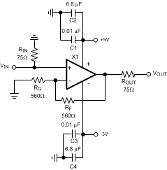
 Figure 32. Typical Video Application
The LMH6703 has been designed to provide excellent performance with production quality video signals in a wide variety of formats such as HDTV and High Resolution VGA. NTSC and PAL performance is nearly flawless with DG of 0.01% and DP of 0.02°. Best performance will be obtained with back terminated loads. The back termination reduces reflections from the transmission line and effectively masks transmission line and other parasitic capacitance from the amplifier output stage. Figure 32 shows a typical configuration for driving 75Ω cable. The amplifier is configured for a gain of two compensating for the 6 dB loss due to ROUT.