ZHCSKK7 December 2019 LMH9226
PRODUCTION DATA.
8.2.2 Detailed Design Procedure
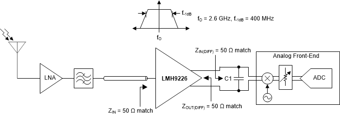
The LMH9226 is a single-to-differential RF gain block amplifier for a 2.6-GHz center frequency application with 400 MHz of the 1-dB bandwidth. Figure 19 shows a single receive channel consisting of a low-noise amplifier (LNA) that sits close to the antenna and drives the signal into a single-ended, 50-Ω coaxial cable that then connects to a transceiver board. The LMH9226 that sits at the transceiver board input converts this single-ended signal received from the coax cable into a differential signal, thereby offering low noise and distortion performance while interfacing with the receiver analog front-end (AFE). The LMH9226 input impedance must be matched to 50 Ω to prevent any signal reflections resulting from the coax cable. The device differential output interfaces directly with the differential input of an AFE. The output matching is optimized for a 50-Ω output at the 2.6-GHz center frequency with 400 MHz of the 1-dB bandwidth. The AFE input impedance must be matched to 50 Ω at 2.6 GHz as well to prevent any ripple in the frequency response.
 Figure 19. LMH9226 in a Receive Application Driving an AFE (ZOUT(DIFF) = 50 Ω)
 For interfacing with a 100-Ω differential input AFE, as shown in Figure 20, an external matching circuitry is needed close to the LMH9226 output. Table 2 lists example recommended component values when transforming the LMH9226 output impedance from 50 Ω to 100 Ω. The component values must be tweaked on the board, depending on the trace length between the matching circuitry and the AFE input to maintain 400 MHz of the 1-dB BW at the 2.6-GHz center frequency. LC component values must be selected with Q(min) > 30 that have a self resonant frequency (SRF) sufficiently higher than the desired frequency of operation. Figure 21 and Figure 22 provide a comparison of device performance when interfacing with a 50-Ω output matching as compared to a 100-Ω output matching. As depicted in Figure 21, the forward path gain (SDS21) is slightly lower for the 100-Ω differential output impedance because of the extra loss in the external matching circuitry.
 Figure 20. LMH9226 in a Receive Application Driving an AFE (ZOUT(DIFF) = 100 Ω)
 Table 2. Output Matching Network Component Values
| COMPONENT | VALUE |
|---|---|
| C2, C3 | 2.2 pF |
| L1 | 6.2 nH |
| L2 | Do not install (DNI) |
Following the recommended RF layout with good quality RF components and local DC bypass capacitors ensures optimal performance is achieved. TI provides various support materials including S-parameter and ADS models to allow the design to be optimized to the application-specific performance needs.