ZHCSH72J september 2011 – may 2023 LMK00301
PRODUCTION DATA
- 1
- 1 特性
- 2 应用
- 3 说明
- 4 Revision History
- 5 Device Comparison
- 6 Pin Configuration and Functions
- 7 Specifications
- 8 Parameter Measurement Information
- 9 Detailed Description
- 10Application and Implementation
- 11Power Supply Recommendations
- 12Layout
- 13Device and Documentation Support
- 14Mechanical, Packaging, and Orderable Information
8.1 Differential Voltage Measurement Terminology
The differential voltage of a differential signal can be described by two different definitions causing confusion when reading data sheets or communicating with other engineers. This section will address the measurement and description of a differential signal so that the reader will be able to understand and discern between the two different definitions when used.
The first definition used to describe a differential signal is the absolute value of the voltage potential between the inverting and non-inverting signal. The symbol for this first measurement is typically VID or VOD depending on if an input or output voltage is being described.
The second definition used to describe a differential signal is to measure the potential of the non-inverting signal with respect to the inverting signal. The symbol for this second measurement is VSS and is a calculated parameter. Nowhere in the IC does this signal exist with respect to ground, it only exists in reference to its differential pair. VSS can be measured directly by oscilloscopes with floating references, otherwise this value can be calculated as twice the value of VOD as described in the first description.
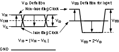
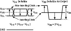
Figure 8-1 illustrates the two different definitions side-by-side for inputs and Figure 8-2 illustrates the two different definitions side-by-side for outputs. The VID (or VOD) definition show the DC levels, VIH and VOL (or VOH and VOL), that the non-inverting and inverting signals toggle between with respect to ground. VSS input and output definitions show that if the inverting signal is considered the voltage potential reference, the non-inverting signal voltage potential is now increasing and decreasing above and below the non-inverting reference. Thus the peak-to-peak voltage of the differential signal can be measured.
VID and VOD are often defined as volts (V) and VSS is often defined as volts peak-to-peak (VPP).
 Figure 8-1 Two Different Definitions for Differential Input Signals
 Figure 8-2 Two Different Definitions for Differential Output Signals
See also AN-912 Common Data Transmission Parameters and their Definitions.