ZHCSH72J september   2011  – may 2023 LMK00301

PRODUCTION DATA  

  1.   1
  2. 特性
  3. 应用
  4. 说明
  5. Revision History
  6. Device Comparison
  7. Pin Configuration and Functions
  8. Specifications
    1. 7.1 Absolute Maximum Ratings
    2. 7.2 ESD Ratings
    3. 7.3 Recommended Operating Conditions
    4. 7.4 Thermal Information
    5. 7.5 Electrical Characteristics
    6. 7.6 Typical Characteristics
  9. Parameter Measurement Information
    1. 8.1 Differential Voltage Measurement Terminology
  10. Detailed Description
    1. 9.1 Overview
    2. 9.2 Functional Block Diagram
    3. 9.3 Feature Description
      1. 9.3.1 VCC and VCCO Power Supplies
    4. 9.4 Device Functional Modes
      1. 9.4.1 Clock Inputs
      2. 9.4.2 Clock Outputs
        1. 9.4.2.1 Reference Output
  11. 10Application and Implementation
    1. 10.1 Application Information
    2. 10.2 Typical Application
      1. 10.2.1 Design Requirements
        1. 10.2.1.1 Driving the Clock Inputs
        2. 10.2.1.2 Crystal Interface
      2. 10.2.2 Detailed Design Procedure
        1. 10.2.2.1 Termination and Use of Clock Drivers
          1. 10.2.2.1.1 Termination for DC Coupled Differential Operation
          2. 10.2.2.1.2 Termination for AC Coupled Differential Operation
          3. 10.2.2.1.3 Termination for Single-Ended Operation
      3. 10.2.3 Application Curves
  12. 11Power Supply Recommendations
    1. 11.1 Power Supply Sequencing
    2. 11.2 Current Consumption and Power Dissipation Calculations
      1. 11.2.1 Power Dissipation Example #1: Separate VCC and VCCO Supplies with Unused Outputs
      2. 11.2.2 Power Dissipation Example #2: Worst-Case Dissipation
    3. 11.3 Power Supply Bypassing
      1. 11.3.1 Power Supply Ripple Rejection
    4. 11.4 Thermal Management
  13. 12Layout
    1. 12.1 Layout Guidelines
    2. 12.2 Layout Example
  14. 13Device and Documentation Support
    1. 13.1 Documentation Support
      1. 13.1.1 Related Documentation
    2. 13.2 接收文档更新通知
    3. 13.3 支持资源
    4. 13.4 Trademarks
    5. 13.5 静电放电警告
    6. 13.6 术语表
  15. 14Mechanical, Packaging, and Orderable Information

封装选项

机械数据 (封装 | 引脚)
散热焊盘机械数据 (封装 | 引脚)
订购信息

Typical Characteristics

Unless otherwise specified: VCC = 3.3 V, VCCO = 3.3 V, TA = 25°C, CLKin driven differentially, input slew rate ≥ 3 V/ns. Consult Table 7-1 at the end of Typical Characteristics for graph notes.
GUID-0A35CAF4-7AF3-4572-B92B-8C9F6C88C087-low.gif
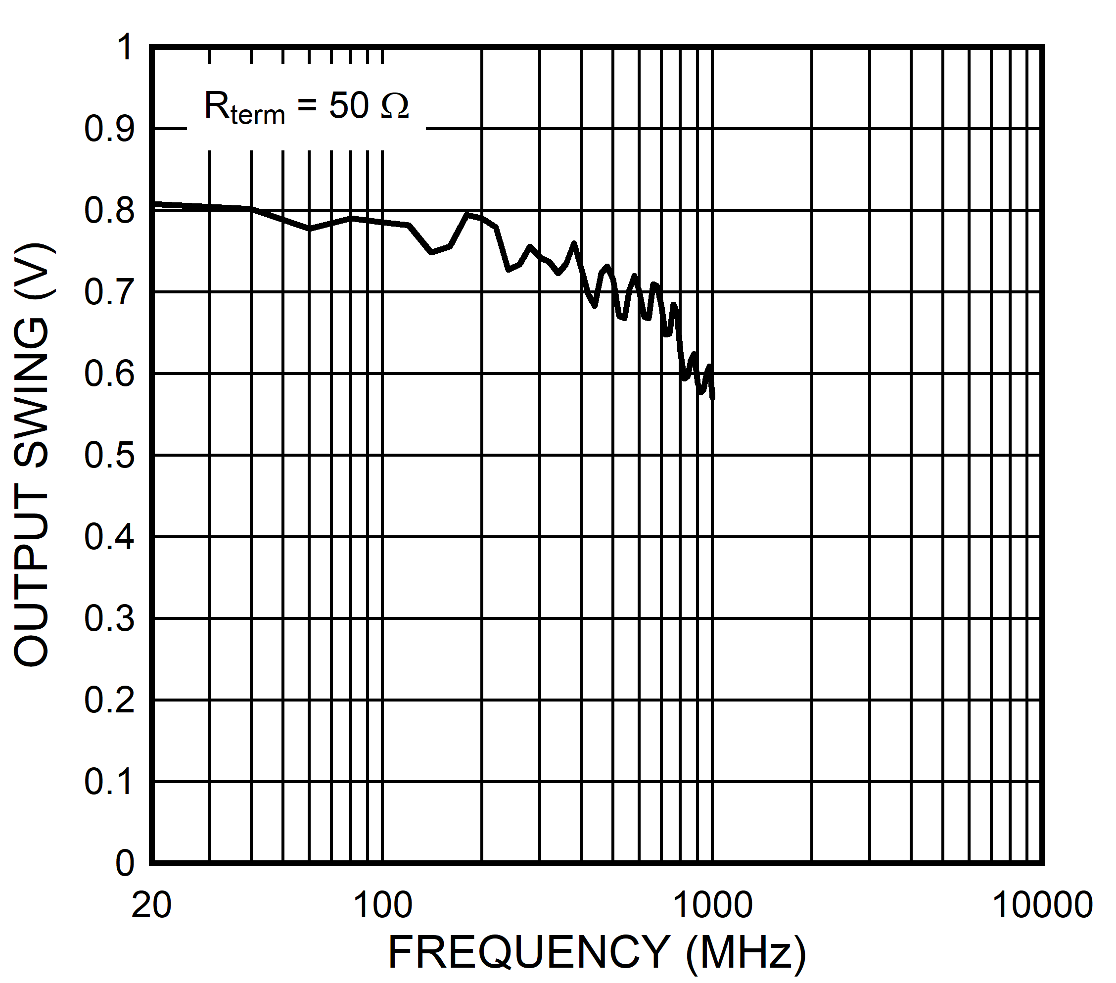
Figure 7-1 LVPECL Output Swing (VOD) vs Frequency
GUID-20230412-SS0I-DHTN-D6WQ-ZLRNV25Z8GSD-low.gif
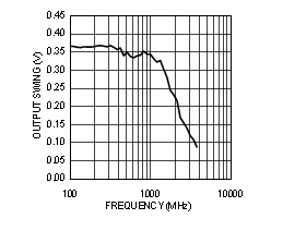
Figure 7-3 HCSL Output Swing (VOD) vs Frequency
GUID-5B68E19A-1C29-4353-864D-AFC9575C60BE-low.gif
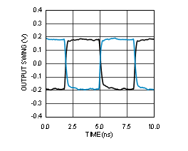
Figure 7-5 LVDS Output Swing at 156.25 MHz
GUID-923A069E-8823-4AB7-A329-BA9BF061C9B4-low.gif
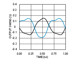
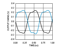
Figure 7-7 LVDS Output Swing at 1.5 GHz
GUID-3662CCA9-FD72-4195-A257-63DC98133610-low.gif
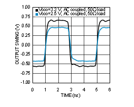
Figure 7-9 LVCMOS Output Swing at 250 MHz
GUID-7FA01866-393A-4EBB-926C-9E814CCF0790-low.gif
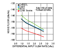
Figure 7-11 Noise Floor vs CLKin Slew Rate at 156.25 MHz
GUID-32971AEF-C69C-4142-90C7-F2A61045E9E3-low.gif
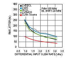
See Note 1 in Graph Notes table
Figure 7-13 RMS Jitter vs CLKin Slew Rate at 100 MHz
GUID-801D4FF7-2F67-456B-8380-D04D43B7B7D2-low.gif
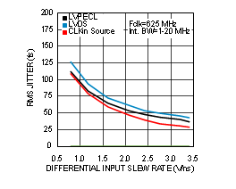
Figure 7-15 RMS Jitter vs CLKin Slew Rate at 625 MHz
GUID-30612515-B733-407F-AA12-746280C34A29-low.gif
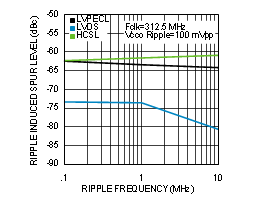
Figure 7-17 PSRR vs Ripple Frequency at 312.5 MHz
GUID-6B1B992F-DB04-499F-9DBE-2343A50AD358-low.gif
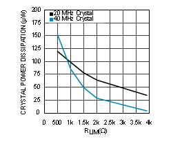
See Notes 2 and 3 in Graph Notes table
Figure 7-19 Crystal Power Dissipation vs RLIM
GUID-07A060CB-E518-4027-9045-6FEBB33DC6F7-low.gif
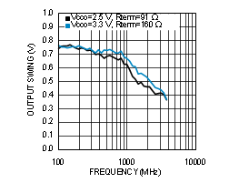
Figure 7-2 LVDS Output Swing (VOD) vs Frequency
GUID-24275D36-2D3C-4C25-A3A1-CAAB530F5CA2-low.gif
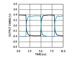
Figure 7-4 LVPECL Output Swing at 156.25 MHz
GUID-1739A76C-765E-4163-9B6D-634593F8D27E-low.gif
Figure 7-6 LVPECL Output Swing at 1.5 GHz
GUID-72328BCD-6319-4838-8AC3-803D9C0BED75-low.gif
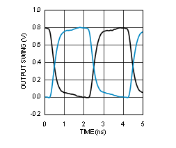
Figure 7-8 HCSL Output Swing at 250 MHz
GUID-A3A8FEEB-0397-4146-9851-8AD96604332A-low.gif
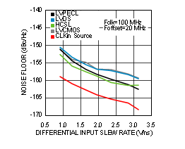
Figure 7-10 Noise Floor vs CLKin Slew Rate at 100 MHz
GUID-298D9390-0803-46EF-B9EE-E4BCA0704A85-low.gif
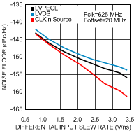
Figure 7-12 Noise Floor vs CLKin Slew Rate at 625 MHz
GUID-6E167C2B-2275-474F-9E6C-41F8C752758C-low.gif
See Note 1 in Graph Notes table
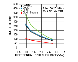
Figure 7-14 RMS Jitter vs CLKin Slew Rate at 156.25 MHz
GUID-1FF12757-42A8-4E56-9D35-CE46C3C3E872-low.gif
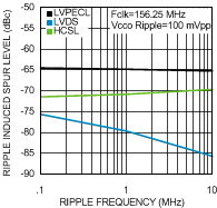
Figure 7-16 PSRR vs Ripple Frequency at 156.25 MHz
GUID-24EC9F86-F46F-4B22-97A9-6C49D2DC6012-low.gif
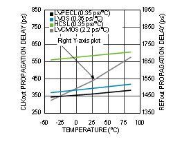
Figure 7-18 Propagation Delay vs Temperature
GUID-BA7A2CFE-0336-4EC3-A2C4-C17E1902A27F-low.gif
See Notes 2 and 3 in Graph Notes table
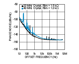
Figure 7-20 LVDS Phase Noise in Crystal Mode
GUID-20230404-SS0I-JFM2-5K7J-WWCWJGCBSCNX-low.png
See Note 1 in Graph Notes table
Figure 7-21 HCSL Phase Noise at 100 MHz
GUID-20230404-SS0I-W8WR-8NJP-RSMHP0ZH0HLK-low.png
See Note 1 in Graph Notes table
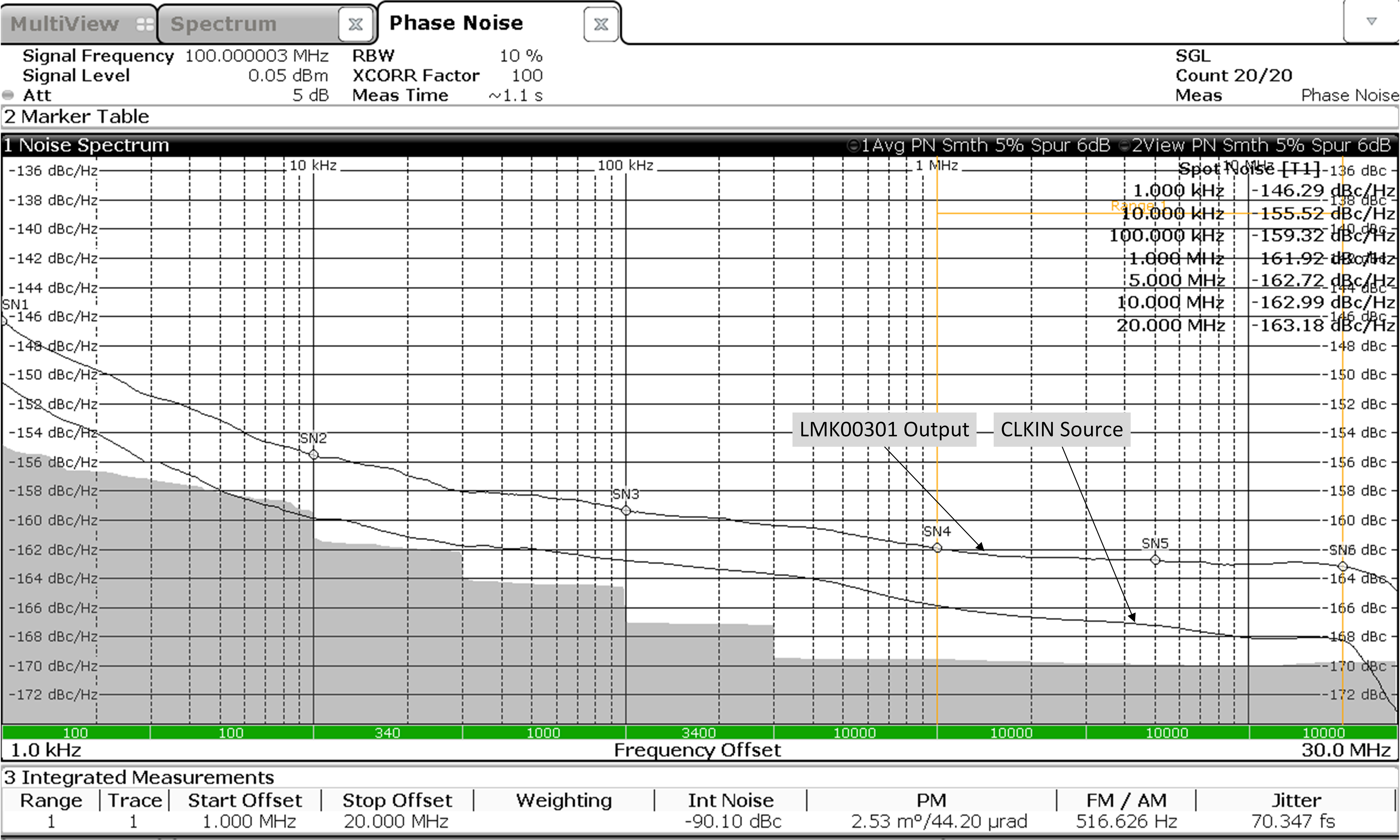
Figure 7-22 LVDS Phase Noise at 100 MHz
GUID-20230404-SS0I-6HJ2-9CNG-NPCFP0FBRQFV-low.png
See Note 1 in Graph Notes table
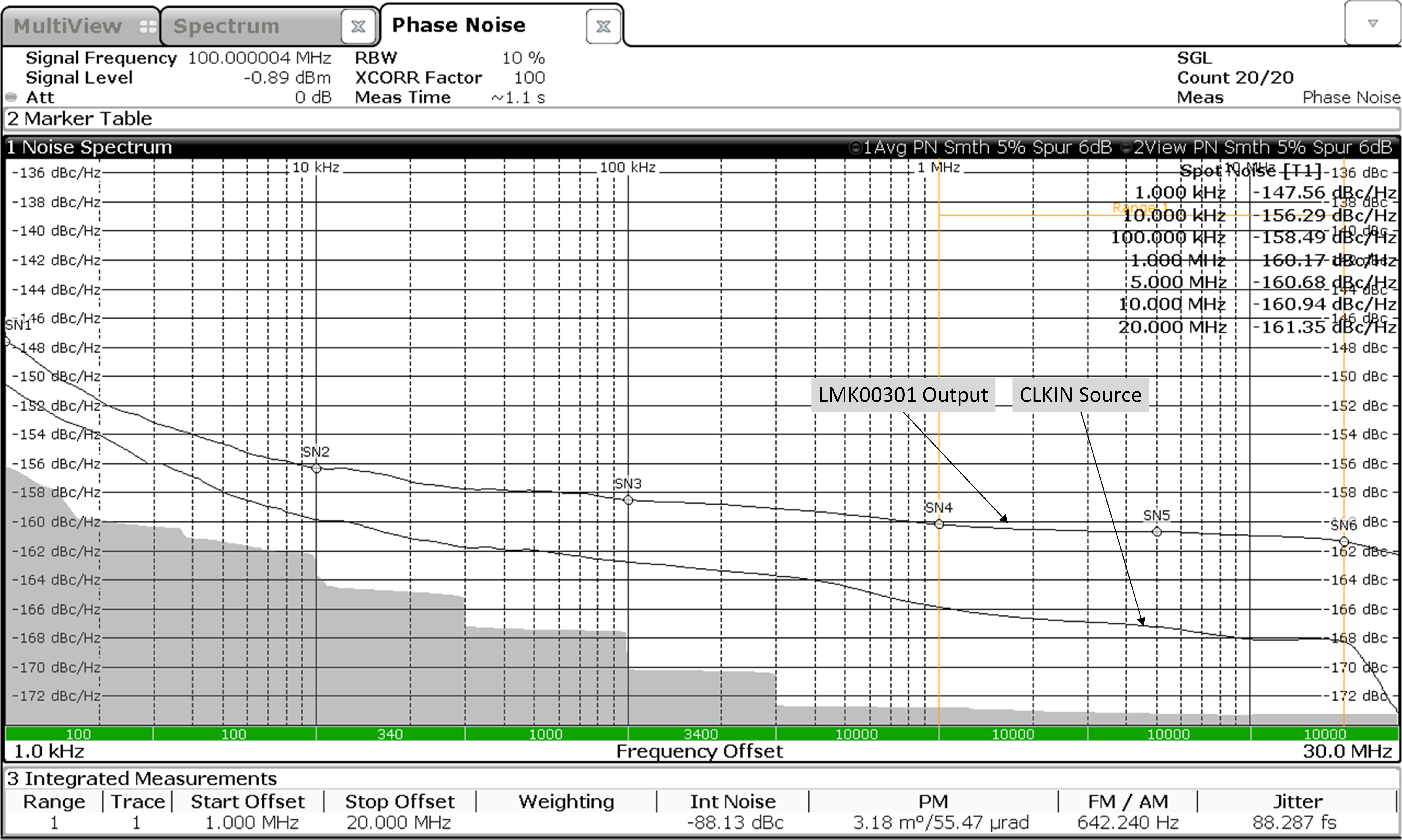
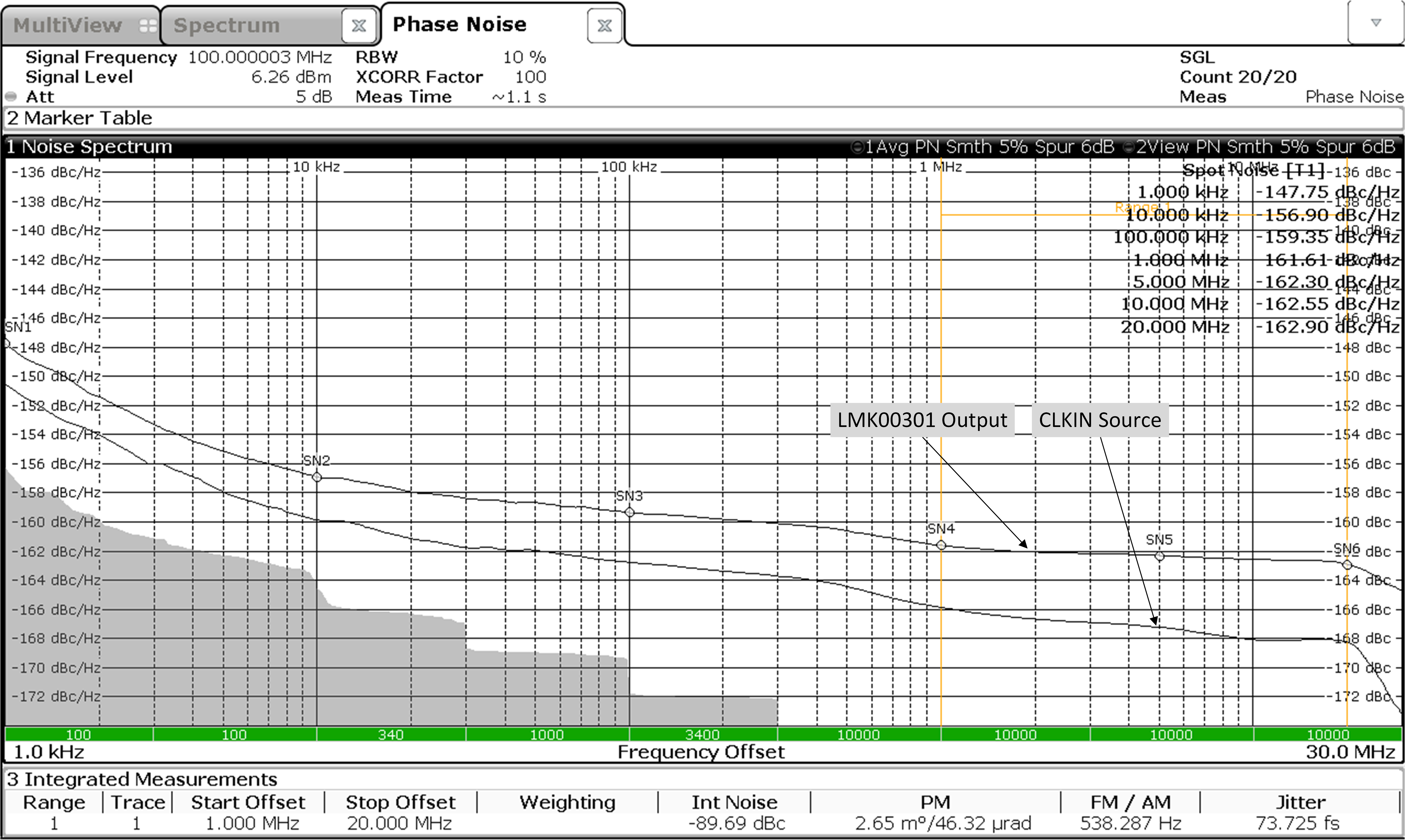
Figure 7-23 LVPECL Phase Noise at 100 MHz
Table 7-1 Graph Notes
NOTE
(1) The typical RMS jitter values in the plots show the total output RMS jitter (JOUT) for each output buffer type and the source clock RMS jitter (JSOURCE). From these values, the Additive RMS Jitter can be calculated as: JADD = SQRT(JOUT2 – JSOURCE2).
(2) 20 MHz crystal characteristics: Abracon ABL series, AT cut, CL = 18 pF , C0 = 4.4 pF measured (7 pF maximum), ESR = 8.5 Ω measured (40 Ω maximum), and Drive Level = 1 mW maximum (100 µW typical).
(3) 40 MHz crystal characteristics: Abracon ABLS2 series, AT cut, CL = 18 pF , C0 = 5 pF measured (7 pF maximum), ESR = 5 Ω measured (40 Ω maximum), and Drive Level = 1 mW maximum (100 µW typical).