ZHCSH72J september 2011 – may 2023 LMK00301
PRODUCTION DATA
- 1
- 1 特性
- 2 应用
- 3 说明
- 4 Revision History
- 5 Device Comparison
- 6 Pin Configuration and Functions
- 7 Specifications
- 8 Parameter Measurement Information
- 9 Detailed Description
- 10Application and Implementation
- 11Power Supply Recommendations
- 12Layout
- 13Device and Documentation Support
- 14Mechanical, Packaging, and Orderable Information
10.2.2.1.2 Termination for AC Coupled Differential Operation
AC coupling allows for shifting the DC bias level (common-mode voltage) when driving different receiver standards. Since AC coupling prevents the driver from providing a DC bias voltage at the receiver, it is important to ensure the receiver is biased to its ideal DC level.
When driving differential receivers with an LVDS driver, the signal may be AC coupled by adding DC blocking capacitors; however the proper DC bias point needs to be established at both the driver side and the receiver side. The recommended termination scheme depends on whether the differential receiver has integrated termination resistors or not.
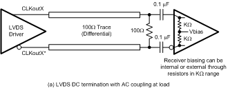
When driving a differential receiver without internal 100 Ω differential termination, the AC coupling capacitors should be placed between the load termination resistor and the receiver to allow a DC path for proper biasing of the LVDS driver. This is shown in Figure 10-10. The load termination resistor and AC coupling capacitors should be placed as close as possible to the receiver inputs to minimize stub length. The receiver can be biased internally or externally to a reference voltage within the receiver’s common mode input range through resistors in the kilo-ohm range.
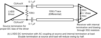
When driving a differential receiver with internal 100 Ω differential termination, a source termination resistor should be placed before the AC coupling capacitors for proper DC biasing of the driver as shown in Figure 10-11. However, with a 100 Ω resistor at the source and the load (that is, double terminated), the equivalent resistance seen by the LVDS driver is 50 Ω which causes the effective signal swing at the input to be reduced by half. If a self-terminated receiver requires input swing greater than 250 mVpp (differential) as well as AC coupling to its inputs, then the LVDS driver with the double-terminated arrangement in Figure 10-11 may not meet the minimum input swing requirement; alternatively, the LVPECL or HCSL output driver format with AC coupling is recommended to meet the minimum input swing required by the self-terminated receiver.
When using AC coupling with LVDS outputs, there may be a start-up delay observed in the clock output due to capacitor charging. The examples in Figure 10-10 and Figure 10-11 use 0.1-μF capacitors, but this value may be adjusted to meet the start-up requirements for the particular application.
 Figure 10-10 Differential LVDS Operation with AC Coupling to Receivers (a.) Without
Internal 100-Ω Termination
 Figure 10-11 Differential LVDS
Operation with AC Coupling to Receivers (b.) With Internal 100-Ω
Termination
Figure 10-11 Differential LVDS
Operation with AC Coupling to Receivers (b.) With Internal 100-Ω
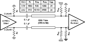
TerminationLVPECL drivers require a DC path to ground. When AC coupling an LVPECL signal use 160-Ω emitter resistors (or 91 Ω for Vcco = 2.5 V) close to the LVPECL driver to provide a DC path to ground as shown in Figure 10-15. For proper receiver operation, the signal should be biased to the DC bias level (common mode voltage) specified by the receiver. The typical DC bias voltage (common mode voltage) for LVPECL receivers is 2 V. Alternatively, a Thevenin equivalent circuit forms a valid termination as shown in Figure 10-12 for Vcco = 3.3 V and 2.5 V. Note: this Thevenin circuit is different from the DC coupled example in Figure 10-9, since the voltage divider is setting the input common-mode voltage of the receiver.
 Figure 10-12 Differential LVPECL Operation, AC Coupling, Thevenin Equivalent