ZHCS808D February 2012 – March 2016 LMK00306
PRODUCTION DATA.
10 Power Supply Recommendations
10.1 Power Supply Sequencing
When powering the Vcc and Vcco pins from separate supply rails, it is recommended for the supplies to reach their regulation point at approximately the same time while ramping up, or reach ground potential at the same time while ramping down. Using simultaneous or ratiometric power supply sequencing prevents internal current flow from Vcc to Vcco pins that could occur when Vcc is powered before Vcco.
10.2 Current Consumption and Power Dissipation Calculations
The current consumption values specified in Electrical Characteristics can be used to calculate the total power dissipation and IC power dissipation for any device configuration. The total VCC core supply current (ICC_TOTAL) can be calculated using Equation 5:
where
- ICC_CORE is the current for core logic and input blocks and depends on selected input (CLKinX or OSCin).
- ICC_BANK_A is the current for Bank A and depends on output type (ICC_PECL, ICC_LVDS, ICC_HCSL, or 0 mA if disabled).
- ICC_BANK_B is the current for Bank B and depends on output type (ICC_PECL, ICC_LVDS, ICC_HCSL, or 0 mA if disabled).
- ICC_CMOS is the current for the LVCMOS output (or 0 mA if REFout is disabled).
Since the output supplies (VCCOA, VCCOB, VCCOC) can be powered from 3 independent voltages, the respective output supply currents (ICCO_BANK_A, ICCO_BANK_B, and ICCO_CMOS) should be calculated separately.
ICCO_BANK for either Bank A or B can be directly taken from the corresponding output supply current spec (ICCO_PECL, ICCO_LVDS, or ICCO_HCSL) provided the output loading matches the specified conditions. Otherwise, ICCO_BANK should be calculated as follows:
where
- IBANK_BIAS is the output bank bias current (fixed value).
- IOUT_LOAD is the DC load current per loaded output pair.
- N is the number of loaded output pairs per bank (N = 0 to 3).
Table 6 shows the typical IBANK_BIAS values and IOUT_LOAD expressions for LVPECL, LVDS, and HCSL.
For LVPECL, it is possible to use a larger termination resistor (RT) to ground instead of terminating with 50 Ω to VTT = Vcco - 2 V; this technique is commonly used to eliminate the extra termination voltage supply (VTT) and potentially reduce device power dissipation at the expense of lower output swing. For example, when Vcco is 3.3 V, a RT value of 160 Ω to ground will eliminate the 1.3 V termination supply without sacrificing much output swing. In this case, the typical IOUT_LOAD is 25 mA, so ICCO_PECL for a fully-loaded bank reduces to 95 mA (vs. 100 mA with 50 Ω resistors to Vcco – 2 V).
Table 6. Typical Output Bank Bias and Load Currents
| CURRENT PARAMETER | LVPECL | LVDS | HCSL |
|---|---|---|---|
| IBANK_BIAS | 20 mA | 17.4 mA | 3.6 mA |
| IOUT_LOAD | (VOH - VTT)/RT + (VOL - VTT)/RT | 0 mA (No DC load current) |
VOH/RT |
Once the current consumption is known for each supply, the total power dissipation (PTOTAL) can be calculated as:
If the device is configured with LVPECL or HCSL outputs, then it is also necessary to calculate the power dissipated in any termination resistors (PRT_ PECL and PRT_HCSL) and in any LVPECL termination voltages (PVTT_PECL). The external power dissipation values can be calculated as follows:
Finally, the IC power dissipation (PDEVICE) can be computed by subtracting the external power dissipation values from PTOTAL as follows:
where
- N1 is the number of LVPECL output pairs with termination resistors to VTT (usually Vcco - 2 V or GND).
- N2 is the number of HCSL output pairs with termination resistors to GND.
10.2.1 Power Dissipation Example: Worst-Case Dissipation
This example shows how to calculate IC power dissipation for a configuration to estimate worst-case power dissipation. In this case, the maximum supply voltage and supply current values specified in Electrical Characteristics are used.
- VCC = VCCO = 3.465 V. Max ICC and ICCO values.
- CLKin0/CLKin0* input is selected.
- Banks A and B are configured for LVPECL: all outputs terminated with 50 Ω to VT = Vcco - 2 V.
- REFout is enabled with 5 pF load.
- TA = 85 °C
Using the power calculations from the previous section and maximum supply current specifications, we can compute PTOTAL and PDEVICE.
- From Equation 5: ICC_TOTAL = 10.5 mA + 22.5 mA + 22.5 mA + 5.5 mA = 61 mA
- From ICCO_PECL max spec: ICCO_BANK_A = ICCO_BANK_B = 115 mA
- From Equation 7: PTOTAL = 3.465 V * (61 mA + 115 mA + 115 mA + 10 mA) = 1043 mW
- From Equation 8: PRT_PECL = ((2.57 V - 1.47 V)2/50 Ω) + ((1.72 V - 1.47 V)2/50 Ω) = 25.5 mW (per output pair)
- From Equation 9: PVTT_PECL = 1.47 V * [ ((2.57 V - 1.47 V) / 50 Ω) + ((1.72 V - 1.47 V) / 50 Ω) ] = 39.5 mW (per output pair)
- From Equation 10: PRT_HCSL = 0 mW (no HCSL outputs)
- From Equation 11: PDEVICE = 1043 mW - (6 * (25.5 mW + 39.5 mW)) - 0 mW = 653 mW
In this worst-case example, the IC device will dissipate about 653 mW or 63% of the total power (1043 mW), while the remaining 37% will be dissipated in the LVPECL emitter resistors (153 mW for 6 pairs) and termination voltage (237 mW into Vcco - 2 V). Based on θJA of 31.8 °C/W, the estimated die junction temperature would be about 21 °C above ambient, or 106 °C when TA = 85 °C.
10.3 Power Supply Bypassing
The Vcc and Vcco power supplies should have a high-frequency bypass capacitor, such as 0.1 uF or 0.01 uF, placed very close to each supply pin. 1 uF to 10 uF decoupling capacitors should also be placed nearby the device between the supply and ground planes. All bypass and decoupling capacitors should have short connections to the supply and ground plane through a short trace or via to minimize series inductance.
10.3.1 Power Supply Ripple Rejection
In practical system applications, power supply noise (ripple) can be generated from switching power supplies, digital ASICs or FPGAs, etc. While power supply bypassing will help filter out some of this noise, it is important to understand the effect of power supply ripple on the device performance. When a single-tone sinusoidal signal is applied to the power supply of a clock distribution device, such as LMK00306, it can produce narrow-band phase modulation as well as amplitude modulation on the clock output (carrier). In the single-side band phase noise spectrum, the ripple-induced phase modulation appears as a phase spur level relative to the carrier (measured in dBc).
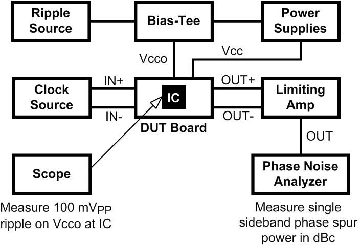
For the LMK00306, power supply ripple rejection, or PSRR, was measured as the single-sideband phase spur level (in dBc) modulated onto the clock output when a ripple signal was injected onto the Vcco supply. The PSRR test setup is shown in Figure 39.
 Figure 39. PSRR Test Setup
A signal generator was used to inject a sinusoidal signal onto the Vcco supply of the DUT board, and the peak-to-peak ripple amplitude was measured at the Vcco pins of the device. A limiting amplifier was used to remove amplitude modulation on the differential output clock and convert it to a single-ended signal for the phase noise analyzer. The phase spur level measurements were taken for clock frequencies of 156.25 MHz and 312.5 MHz under the following power supply ripple conditions:
- Ripple amplitude: 100 mVpp on Vcco = 2.5 V
- Ripple frequencies: 100 kHz, 1 MHz, and 10 MHz
Assuming no amplitude modulation effects and small index modulation, the peak-to-peak deterministic jitter (DJ) can be calculated using the measured single-sideband phase spur level (PSRR) as follows:
The “PSRR vs. Ripple Frequency” plots in Typical Characteristics show the ripple-induced phase spur levels for the differential output types at 156.25 MHz and 312.5 MHz . The LMK00306 exhibits very good and well-behaved PSRR characteristics across the ripple frequency range for all differential output types. The phase spur levels for LVPECL are below -64 dBc at 156.25 MHz and below -62 dBc at 312.5 MHz. Using Equation 12, these phase spur levels translate to Deterministic Jitter values of 2.57 ps pk-pk at 156.25 MHz and 1.62 ps pk-pk at 312.5 MHz. Testing has shown that the PSRR performance of the device improves for Vcco = 3.3 V under the same ripple amplitude and frequency conditions.
10.4 Thermal Management
Power dissipation in the LMK00306 device can be high enough to require attention to thermal management. For reliability and performance reasons the die temperature should be limited to a maximum of 125 °C. That is, as an estimate, TA (ambient temperature) plus device power dissipation times RθJA should not exceed 125 °C.
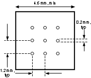
The package of the device has an exposed pad that provides the primary heat removal path as well as excellent electrical grounding to the printed circuit board. To maximize the removal of heat from the package a thermal land pattern including multiple vias to a ground plane must be incorporated on the PCB within the footprint of the package. The exposed pad must be soldered down to ensure adequate heat conduction out of the package.
A recommended land and via pattern is shown in Figure 40. More information on soldering WQFN packages can be obtained at: http://www.ti.com/packaging.
 Figure 40. Recommended Land and Via Pattern
To minimize junction temperature it is recommended that a simple heat sink be built into the PCB (if the ground plane layer is not exposed). This is done by including a copper area of about 2 square inches on the opposite side of the PCB from the device. This copper area may be plated or solder coated to prevent corrosion but should not have conformal coating (if possible), which could provide thermal insulation. The vias shown in Figure 40 should connect these top and bottom copper layers and to the ground layer. These vias act as “heat pipes” to carry the thermal energy away from the device side of the board to where it can be more effectively dissipated.