ZHCSCZ6C December 2013 – July 2021 LMK00338
PRODUCTION DATA
10.3 Thermal Management
Power dissipation in the LMK00338 device can be high enough to require attention to thermal management. For reliability and performance reasons the die temperature should be limited to a maximum of 125°C. That is, as an estimate, TA (ambient temperature) plus device power dissipation times RθJA should not exceed 125°C.
The package of the device has an exposed pad that provides the primary heat removal path as well as excellent electrical grounding to the printed-circuit board. To maximize the removal of heat from the package a thermal land pattern including multiple vias to a ground plane must be incorporated on the PCB within the footprint of the package. The exposed pad must be soldered down to ensure adequate heat conduction out of the package.
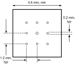
A recommended land and via pattern is shown in Figure 10-2. More information on soldering WQFN packages can be obtained at: https://www.ti.com/packaging.
 Figure 10-2 Recommended Land and Via Pattern
To minimize junction temperature, TI recommends building a simple heat sink into the PCB (if the ground plane layer is not exposed). This is done by including a copper area of about 2 square inches on the opposite side of the PCB from the device. This copper area may be plated or solder coated to prevent corrosion but should not have conformal coating (if possible), which could provide thermal insulation. The vias shown in Figure 10-2 should connect these top and bottom copper layers and to the ground layer. These vias act as heat pipes to carry the thermal energy away from the device side of the board to where it can be more effectively dissipated.