ZHCSCY6A June 2014 – July 2014 LMK00804B
PRODUCTION DATA.
- 1 特性
- 2 应用
- 3 说明
- 4 简化电路原理图
- 5 修订历史记录
- 6 Device Comparison Table
- 7 Pin Configuration and Functions
-
8 Specifications
- 8.1 Pin Characteristics
- 8.2 Absolute Maximum Ratings
- 8.3 Handling Ratings
- 8.4 Recommended Operating Conditions
- 8.5 Thermal Information
- 8.6 Power Supply Characteristics
- 8.7 LVCMOS / LVTTL DC Characteristics
- 8.8 Differential Input DC Characteristics
- 8.9 Electrical Characteristics (VDDO = 3.3 V ± 5%)
- 8.10 Electrical Characteristics (VDDO = 2.5 V ± 5%)
- 8.11 Electrical Characteristics (VDDO = 1.8 V ± 0.15 V)
- 8.12 Electrical Characteristics (VDDO = 1.5 V ± 5%)
- 8.13 Typical Characteristics
- 9 Parameter Measurement Information
- 10Detailed Description
- 11Applications and Implementation
- 12Power Supply Recommendations
- 13Layout
- 14器件和文档支持
- 15机械封装和可订购信息
12 Power Supply Recommendations
12.1 Power Supply Considerations
While there is no strict power supply sequencing requirement, it is generally best practice to sequence the core supply voltage (VDD) before the output supply voltage (VDDO).
12.1.1 Power-Supply Filtering
High-performance clock buffers are sensitive to noise on the power supply, which can dramatically increase the additive jitter of the buffer. Thus, it is essential to reduce noise from the system power supply, especially when jitter or phase noise is critical to applications.
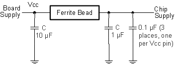
Use of filter capacitors eliminates the low-frequency noise from power supply, where the bypass capacitors provide the very low-impedance path for high-frequency noise and guard the power-supply system against induced fluctuations. The bypass capacitors also provide instantaneous current surges as required by the device, and should have low ESR. To use the bypass capacitors properly, place them very close to the power supply terminals and lay out traces with short loops to minimize inductance. TI recommends to adding as many high-frequency (for example, 0.1 µF) bypass capacitors as there are supply terminals in the package. It is recommended, but not required, to insert a ferrite bead between the board power supply and the chip power supply to isolate the high-frequency switching noises generated by the clock driver, preventing them from leaking into the board supply. Choosing an appropriate ferrite bead with very low DC resistance is important, because it is imperative to provide adequate isolation between the board supply and the chip supply. It is also imperative to maintain a voltage at the supply terminals that is greater than the minimum voltage required for proper operation.
 Figure 20. Power-Supply Decoupling
12.1.2 Thermal Management
For reliability and performance reasons, limit the die temperature to a maximum of 125°C. That is, as an estimate, TA (ambient temperature) plus device power consumption times θJA should not exceed 125°C.
Assuming the conditions in the Power Considerations section and operating at an ambient temperature of 70°C with all outputs loaded, here is an estimate of the LMK00804B junction temperature:
Here are some recommendations for improving heat flow away from the die:
- Use multi-layer boards
- Specify a higher copper thickness for the board
- Increase the number of vias from the top level ground plane under and around the device to internal layers and to the bottom layer with as much copper area flow on each level as possible
- Apply air flow
- Leave unused outputs floating