ZHCSHU9K September 2011 – December 2023 LMK03806
PRODUCTION DATA
- 1
- 1 特性
- 2 应用
- 3 描述
- 4 Pin Configuration and Functions
- 5 Specifications
- 6 Parameter Measurement Information
-
7 Detailed Description
- 7.1 Overview
- 7.2 Functional Block Diagrams
- 7.3 Features Description
- 7.4 Device Functional Modes
- 7.5 Programming
-
8 Application and Implementation
- 8.1 Application Information
- 8.2 Typical Application
- 8.3 System Examples
- 8.4 Best Design Practices
- 8.5 Power Supply Recommendations
- 8.6 Layout
- 9 Device and Documentation Support
-
10Register Maps
- 10.1 Default Device Register Settings After Power On Reset
- 10.2 Register R0 TO R5
- 10.3 Registers R6 TO R8
- 10.4 REGISTER R9
- 10.5 REGISTER R10
- 10.6 REGISTER R11
- 10.7 REGISTER R12
- 10.8 REGISTER R13
- 10.9 REGISTER 14
- 10.10 REGISTER 16
- 10.11 REGISTER 24
- 10.12 REGISTER 26
- 10.13 REGISTER 28
- 10.14 REGISTER 29
- 10.15 REGISTER 30
- 10.16 REGISTER 31
- 11Revision History
- 12Mechanical, Packaging, and Orderable Information
4 Pin Configuration and Functions
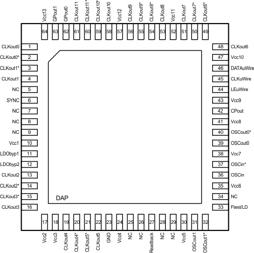
 Figure 4-1 NKD Package64-Pin WQFNTop View
Table 4-1 Pin Functions
| PIN | I/O | TYPE | DESCRIPTION | |
|---|---|---|---|---|
| NAME | NO. | |||
| CLKout0, CLKout0* | 1, 2 | O | Programmable | Clock output 0 (clock group 0). |
| CLKout1*, CLKout1 | 3, 4 | O | Programmable | Clock output 1 (clock group 0). |
| CLKout2, CLKout2* | 13, 14 | O | Programmable | Clock output 2 (clock group 1). |
| CLKout3*, CLKout3 | 15, 16 | O | Programmable | Clock output 3 (clock group 1). |
| CLKout4, CLKout4* | 19, 20 | O | Programmable | Clock output 4 (clock group 2). |
| CLKout5*, CLKout5 | 21, 22 | O | Programmable | Clock output 5 (clock group 2). |
| CLKout6, CLKout6* | 48, 49 | O | Programmable | Clock output 6 (clock group 3). |
| CLKout7*, CLKout7 | 50, 51 | O | Programmable | Clock output 7 (clock group 3). |
| CLKout8, CLKout8* | 53, 54 | O | Programmable | Clock output 8 (clock group 4). |
| CLKout9*, CLKout9 | 55, 56 | O | Programmable | Clock output 9 (clock group 4). |
| CLKout10, CLKout10* | 58, 59 | O | Programmable | Clock output 10 (clock group 5). |
| CLKout11*, CLKout11 | 60, 61 | O | Programmable | Clock output 11 (clock group 5). |
| CLKuWire | 45 | I | CMOS | MICROWIRE Clock Input. |
| CPout | 42 | O | ANLG | Charge pump output. |
| DAP | DAP | — | GND | DIE ATTACH PAD, connect to GND. |
| DATAuWire | 46 | I | CMOS | MICROWIRE Data Input. |
| Ftest/LD | 33 | O | Programmable | Multiplexed Lock Detect and Test output pin. |
| GND | 23 | — | PWR | Ground |
| GPout0, GPout1 | 62, 63 | O | CMOS | These pins can be programmed for general purpose output. |
| LDObyp1 | 11 | — | ANLG | LDO Bypass, bypassed to ground with 10 µF capacitor. |
| LDObyp2 | 12 | — | ANLG | LDO Bypass, bypassed to ground with a 0.1 µF capacitor. |
| LEuWire | 44 | I | CMOS | MICROWIRE Latch Enable Input. |
| NC | 5, 7, 8, 9, 25, 26, 28,29, 34 | — | Do Not Connect | These pins must be left floating. Do NOT ground. |
| OSCout1, OSCout1* | 31, 32 | O | LVPECL | Buffered output 1 of OSCin port. |
| OSCin, OSCin* | 36, 37 | I | ANLG |
Reference input to PLL. Reference input may be: A Crystal for use with the internal crystal oscillator circuit. A XO, TCXO, or other external clock. Must be AC Coupled. |
| OSCout0, OSCout0* | 39, 40 | O | Programmable | Buffered output 0 of OSCin port. |
| Readback | 27 | O | CMOS | Pin that can be used to readback register information. |
| SYNC | 6 | I | CMOS | Clock synchronization input. |
| Vcc1 | 10 | — | PWR | Power supply for VCO LDO. |
| Vcc2 | 17 | — | PWR | Power supply for clock group 1: CLKout2 and CLKout3. |
| Vcc3 | 18 | — | PWR | Power supply for clock group 2: CLKout4 and CLKout5. |
| Vcc4 | 24 | — | PWR | Power supply for digital. |
| Vcc5 | 30 | — | PWR | Power supply for clock inputs. |
| Vcc6 | 35 | — | PWR | Power supply. No bypassing required on this pin. |
| Vcc7 | 38 | — | PWR | Power supply for OSCin port. |
| Vcc8 | 41 | — | PWR | Power supply for PLL charge pump. |
| Vcc9 | 43 | — | PWR | Power supply for PLL. |
| Vcc10 | 47 | — | PWR | Power supply for clock group 3: CLKout6 and CLKout7. |
| Vcc11 | 52 | — | PWR | Power supply for clock group 4: CLKout8 and CLKout9. |
| Vcc12 | 57 | — | PWR | Power supply for clock group 5: CLKout10 and CLKout11. |
| Vcc13 | 64 | — | PWR | Power supply for clock group 0: CLKout0 and CLKout1. |