ZHCSEI4C July   2012  – January 2016 LMK04816

PRODUCTION DATA.  

  1. 特性
  2. 应用
  3. 说明
  4. 修订历史记录
  5. Pin Configuration and Functions
  6. Specifications
    1. 6.1 Absolute Maximum Ratings
    2. 6.2 ESD Ratings
    3. 6.3 Recommended Operating Conditions
    4. 6.4 Thermal Information
    5. 6.5 Electrical Characteristics
    6. 6.6 Timing Requirements
    7. 6.7 Typical Characteristics: Clock Output AC Charcteristics
  7. Parameter Measurement Information
    1. 7.1 Charge Pump Current Specification Definitions
      1. 7.1.1 Charge-Pump Output Current Magnitude Variation vs Charge-Pump Output Voltage
      2. 7.1.2 Charge-Pump Sink Current vs Charge-Pump Output Source Current Mismatch
      3. 7.1.3 Charge-Pump Output Current Magnitude Variation vs Temperature
    2. 7.2 Differential Voltage Measurement Terminology
  8. Detailed Description
    1. 8.1 Overview
      1. 8.1.1  System Architecture
      2. 8.1.2  PLL1 Redundant Reference Inputs (CLKin0/CLKin0*, CLKin1/CLKin1*, and CLKin2/CLKin2*)
      3. 8.1.3  PLL1 Tunable Crystal Support
      4. 8.1.4  VCXO and CRYSTAL-Buffered Outputs
      5. 8.1.5  Frequency Holdover
      6. 8.1.6  Integrated Loop Filter Poles
      7. 8.1.7  Internal VCO
      8. 8.1.8  External VCO Mode
      9. 8.1.9  Clock Distribution
        1. 8.1.9.1 CLKout Divider
        2. 8.1.9.2 CLKout Delay
        3. 8.1.9.3 Programmable Output Type
        4. 8.1.9.4 Clock Output Synchronization
      10. 8.1.10 0-Delay
      11. 8.1.11 Default Start-Up Clocks
      12. 8.1.12 Status Pins
      13. 8.1.13 Register Readback
    2. 8.2 Functional Block Diagram
    3. 8.3 Feature Description
      1. 8.3.1  Serial MICROWIRE Timing Diagram
      2. 8.3.2  Advanced MICROWIRE Timing Diagrams
        1. 8.3.2.1 Three Extra Clocks or Double Program
        2. 8.3.2.2 Three Extra Clocks with LEuWire High
        3. 8.3.2.3 Readback
      3. 8.3.3  Inputs and Outputs
        1. 8.3.3.1 PLL1 Reference Inputs (CLKin0, CLKin1, and CLKin2)
        2. 8.3.3.2 PLL2 OSCin and OSCin* Port
        3. 8.3.3.3 Crystal Oscillator
      4. 8.3.4  Input Clock Switching
        1. 8.3.4.1 Input Clock Switching - Manual Mode
        2. 8.3.4.2 Input Clock Switching - Pin Select Mode
          1. 8.3.4.2.1 Pin Select Mode and Host
          2. 8.3.4.2.2 Switch Event Without Holdover
          3. 8.3.4.2.3 Switch Event With Holdover
        3. 8.3.4.3 Input Clock Switching - Automatic Mode
        4. 8.3.4.4 Input Clock Switching - Automatic Mode With Pin Select
      5. 8.3.5  Holdover Mode
        1. 8.3.5.1 Enable Holdover
        2. 8.3.5.2 Entering Holdover
        3. 8.3.5.3 During Holdover
        4. 8.3.5.4 Exiting holdover
        5. 8.3.5.5 Holdover Frequency Accuracy and DAC Performance
        6. 8.3.5.6 Holdover Mode - Automatic Exit of Holdover
      6. 8.3.6  PLLs
        1. 8.3.6.1 PLL1
        2. 8.3.6.2 PLL2
          1. 8.3.6.2.1 PLL2 Frequency Doubler
        3. 8.3.6.3 Digital Lock Detect
      7. 8.3.7  Status Pins
        1. 8.3.7.1 Logic Low
        2. 8.3.7.2 Digital Lock Detect
        3. 8.3.7.3 Holdover Status
        4. 8.3.7.4 DAC
        5. 8.3.7.5 PLL Divider Outputs
        6. 8.3.7.6 CLKinX_LOS
        7. 8.3.7.7 CLKinX Selected
        8. 8.3.7.8 MICROWIRE Readback
      8. 8.3.8  VCO
      9. 8.3.9  Clock Distribution
        1. 8.3.9.1 Fixed Digital Delay
          1. 8.3.9.1.1 Fixed Digital Delay - Example
        2. 8.3.9.2 Clock Output Synchronization (SYNC)
          1. 8.3.9.2.1 Effect of SYNC
          2. 8.3.9.2.2 Methods of Generating SYNC
          3. 8.3.9.2.3 Avoiding Clock Output Interruption due to SYNC
          4. 8.3.9.2.4 SYNC Timing
          5. 8.3.9.2.5 Dynamically Programming Digital Delay
            1. 8.3.9.2.5.1 Absolute versus Relative Dynamic Digital Delay
            2. 8.3.9.2.5.2 Dynamic Digital Delay and 0-Delay Mode
            3. 8.3.9.2.5.3 SYNC and Minimum Step Size
            4. 8.3.9.2.5.4 Programming Overview
            5. 8.3.9.2.5.5 Internal Dynamic Digital Delay Timing
            6. 8.3.9.2.5.6 Other Timing Requirements
            7. 8.3.9.2.5.7 Absolute Dynamic Digital Delay
              1. 8.3.9.2.5.7.1 Absolute Dynamic Digital Delay - Example
            8. 8.3.9.2.5.8 Relative Dynamic Digital Delay
              1. 8.3.9.2.5.8.1 Relative Dynamic Digital Delay - Example
      10. 8.3.10 0-Delay Mode
    4. 8.4 Device Functional Modes
      1. 8.4.1 Mode Selection
      2. 8.4.2 Operating Modes
        1. 8.4.2.1 Dual PLL
        2. 8.4.2.2 0-Delay Dual PLL
        3. 8.4.2.3 Single PLL
        4. 8.4.2.4 0-delay Single PLL
        5. 8.4.2.5 Clock Distribution
    5. 8.5 Programming
      1. 8.5.1 Special Programming Case for R0 to R5 for CLKoutX_Y_DIV and CLKoutX_Y_DDLY
        1. 8.5.1.1 Example
      2. 8.5.2 Recommended Programming Sequence
        1. 8.5.2.1 Overview
      3. 8.5.3 Readback
        1. 8.5.3.1 Readback - Example
    6. 8.6 Register Maps
      1. 8.6.1 Register Map and Readback Register Map
      2. 8.6.2 Default Device Register Settings After Power On Reset
      3. 8.6.3 Register Descriptions
        1. 8.6.3.1  Registers R0 to R5
          1. 8.6.3.1.1 CLKoutX_Y_PD, Powerdown CLKoutX_Y Output Path
          2. 8.6.3.1.2 CLKoutX_Y_OSCin_Sel, Clock group source
          3. 8.6.3.1.3 CLKoutY_ADLY_SEL[29], CLKoutX_ADLY_SEL[28], Select Analog Delay
          4. 8.6.3.1.4 CLKoutX_Y_DDLY, Clock Channel Digital Delay
          5. 8.6.3.1.5 RESET
          6. 8.6.3.1.6 POWERDOWN
          7. 8.6.3.1.7 CLKoutX_Y_HS, Digital Delay Half Shift
          8. 8.6.3.1.8 CLKoutX_Y_DIV, Clock Output Divide
        2. 8.6.3.2  Registers R6 TO R8
          1. 8.6.3.2.1 CLKoutX_TYPE
          2. 8.6.3.2.2 CLKoutX_Y_ADLY
        3. 8.6.3.3  Register R10
          1. 8.6.3.3.1 OSCout0_TYPE
          2. 8.6.3.3.2 EN_OSCout0, OSCout0 Output Enable
          3. 8.6.3.3.3 OSCout0_MUX, Clock Output Mux
          4. 8.6.3.3.4 PD_OSCin, OSCin Powerdown Control
          5. 8.6.3.3.5 OSCout_DIV, Oscillator Output Divide
          6. 8.6.3.3.6 VCO_MUX
          7. 8.6.3.3.7 EN_FEEDBACK_MUX
          8. 8.6.3.3.8 VCO_DIV, VCO Divider
          9. 8.6.3.3.9 FEEDBACK_MUX
        4. 8.6.3.4  Register R11
          1. 8.6.3.4.1 MODE: Device Mode
          2. 8.6.3.4.2 EN_SYNC, Enable Synchronization
          3. 8.6.3.4.3 NO_SYNC_CLKoutX_Y
          4. 8.6.3.4.4 SYNC_CLKin2_MUX
          5. 8.6.3.4.5 SYNC_QUAL
          6. 8.6.3.4.6 SYNC_POL_INV
          7. 8.6.3.4.7 SYNC_EN_AUTO
          8. 8.6.3.4.8 SYNC_TYPE
          9. 8.6.3.4.9 EN_PLL2_XTAL
        5. 8.6.3.5  Register R12
          1. 8.6.3.5.1 LD_MUX
          2. 8.6.3.5.2 LD_TYPE
          3. 8.6.3.5.3 SYNC_PLLX_DLD
          4. 8.6.3.5.4 EN_TRACK
          5. 8.6.3.5.5 HOLDOVER_MODE
        6. 8.6.3.6  Register R13
          1. 8.6.3.6.1 HOLDOVER_MUX
          2. 8.6.3.6.2 HOLDOVER_TYPE
          3. 8.6.3.6.3 Status_CLKin1_MUX
          4. 8.6.3.6.4 Status_CLKin0_TYPE
          5. 8.6.3.6.5 DISABLE_DLD1_DET
          6. 8.6.3.6.6 Status_CLKin0_MUX
          7. 8.6.3.6.7 CLKin_SELECT_MODE
          8. 8.6.3.6.8 CLKin_Sel_INV
          9. 8.6.3.6.9 EN_CLKinX
        7. 8.6.3.7  Register 14
          1. 8.6.3.7.1 LOS_TIMEOUT
          2. 8.6.3.7.2 EN_LOS
          3. 8.6.3.7.3 Status_CLKin1_TYPE
          4. 8.6.3.7.4 CLKinX_BUF_TYPE, PLL1 CLKinX/CLKinX* Buffer Type
          5. 8.6.3.7.5 DAC_HIGH_TRIP
          6. 8.6.3.7.6 DAC_LOW_TRIP
          7. 8.6.3.7.7 EN_VTUNE_RAIL_DET
        8. 8.6.3.8  Register 15
          1. 8.6.3.8.1 MAN_DAC
          2. 8.6.3.8.2 EN_MAN_DAC
          3. 8.6.3.8.3 HOLDOVER_DLD_CNT
          4. 8.6.3.8.4 FORCE_HOLDOVER
        9. 8.6.3.9  Register 16
          1. 8.6.3.9.1 XTAL_LVL
        10. 8.6.3.10 Register 23
          1. 8.6.3.10.1 DAC_CNT
        11. 8.6.3.11 REGISTER 24
          1. 8.6.3.11.1 PLL2_C4_LF, PLL2 Integrated Loop Filter Component
          2. 8.6.3.11.2 PLL2_C3_LF, PLL2 Integrated Loop Filter Component
          3. 8.6.3.11.3 PLL2_R4_LF, PLL2 Integrated Loop Filter Component
          4. 8.6.3.11.4 PLL2_R3_LF, PLL2 Integrated Loop Filter Component
          5. 8.6.3.11.5 PLL1_N_DLY
          6. 8.6.3.11.6 PLL1_R_DLY
          7. 8.6.3.11.7 PLL1_WND_SIZE
        12. 8.6.3.12 Register 25
          1. 8.6.3.12.1 DAC_CLK_DIV
          2. 8.6.3.12.2 PLL1_DLD_CNT
        13. 8.6.3.13 Register 26
          1. 8.6.3.13.1 PLL2_WND_SIZE
          2. 8.6.3.13.2 EN_PLL2_REF_2X, PLL2 Reference Frequency Doubler
          3. 8.6.3.13.3 PLL2_CP_POL, PLL2 Charge Pump Polarity
          4. 8.6.3.13.4 PLL2_CP_GAIN, PLL2 Charge Pump Current
          5. 8.6.3.13.5 PLL2_DLD_CNT
          6. 8.6.3.13.6 PLL2_CP_TRI, PLL2 Charge Pump Tri-State
        14. 8.6.3.14 Register 27
          1. 8.6.3.14.1 PLL1_CP_POL, PLL1 Charge Pump Polarity
          2. 8.6.3.14.2 PLL1_CP_GAIN, PLL1 Charge Pump Current
          3. 8.6.3.14.3 CLKinX_PreR_DIV
          4. 8.6.3.14.4 PLL1_R, PLL1 R Divider
          5. 8.6.3.14.5 PLL1_CP_TRI, PLL1 Charge Pump Tri-State
        15. 8.6.3.15 Register 28
          1. 8.6.3.15.1 PLL2_R, PLL2 R Divider
          2. 8.6.3.15.2 PLL1_N, PLL1 N Divider
        16. 8.6.3.16 Register 29
          1. 8.6.3.16.1 OSCin_FREQ, PLL2 Oscillator Input Frequency Register
          2. 8.6.3.16.2 PLL2_FAST_PDF, High PLL2 Phase Detector Frequency
          3. 8.6.3.16.3 PLL2_N_CAL, PLL2 N Calibration Divider
        17. 8.6.3.17 Register 30
          1. 8.6.3.17.1 PLL2_P, PLL2 N Prescaler Divider
          2. 8.6.3.17.2 PLL2_N, PLL2 N Divider
        18. 8.6.3.18 Register 31
          1. 8.6.3.18.1 READBACK_LE
          2. 8.6.3.18.2 READBACK_ADDR
          3. 8.6.3.18.3 uWire_LOCK
  9. Application and Implementation
    1. 9.1 Application Information
      1. 9.1.1 Loop Filter
        1. 9.1.1.1 PLL1
        2. 9.1.1.2 PLL2
      2. 9.1.2 Driving CLKin and OSCin Inputs
        1. 9.1.2.1 Driving CLKin Pins With a Differential Source
        2. 9.1.2.2 Driving CLKin Pins With a Single-Ended Source
      3. 9.1.3 Termination and Use of Clock Output (Drivers)
        1. 9.1.3.1 Termination for DC-Coupled Differential Operation
        2. 9.1.3.2 Termination for AC-Coupled Differential Operation
        3. 9.1.3.3 Termination for Single-Ended Operation
      4. 9.1.4 Frequency Planning With the LMK04816
      5. 9.1.5 PLL Programming
        1. 9.1.5.1 Example PLL2 N Divider Programming
      6. 9.1.6 Digital Lock Detect Frequency Accuracy
        1. 9.1.6.1 Minimum Lock Time Calculation Example
      7. 9.1.7 Calculating Dynamic Digital Delay Values for Any Divide
        1. 9.1.7.1 Example
      8. 9.1.8 Optional Crystal Oscillator Implementation (OSCin and OSCin*)
    2. 9.2 Typical Application
      1. 9.2.1 Design Requirements
      2. 9.2.2 Detailed Design Procedure
        1. 9.2.2.1 Device Selection
          1. 9.2.2.1.1 Clock Architect
          2. 9.2.2.1.2 Clock Design Tool
          3. 9.2.2.1.3 Calculation Using LCM
        2. 9.2.2.2 Device Configuration
          1. 9.2.2.2.1 PLL LO Reference
          2. 9.2.2.2.2 POR Clock
        3. 9.2.2.3 PLL Loop Filter Design
          1. 9.2.2.3.1 PLL1 Loop Filter Design
          2. 9.2.2.3.2 PLL2 Loop Filter Design
        4. 9.2.2.4 Clock Output Assignment
        5. 9.2.2.5 Other Device Specific Configuration
          1. 9.2.2.5.1 Digital Lock Detect
          2. 9.2.2.5.2 Holdover
        6. 9.2.2.6 Device Programming
      3. 9.2.3 Application Curve
    3. 9.3 System Examples
  10. 10Power Supply Recommendations
    1. 10.1 Pin Connection Recommendations
      1. 10.1.1 Vcc Pins and Decoupling
        1. 10.1.1.1 Vcc2, Vcc3, Vcc10, Vcc11, Vcc12, Vcc13 (CLKout Vccs)
        2. 10.1.1.2 Vcc1 (VCO), Vcc4 (Digital), and Vcc9 (PLL2)
        3. 10.1.1.3 Vcc6 (PLL1 Charge Pump) and Vcc8 (PLL2 Charge Pump)
        4. 10.1.1.4 Vcc5 (CLKin), Vcc7 (OSCin and OSCout0)
      2. 10.1.2 LVPECL Outputs
      3. 10.1.3 Unused Clock Outputs
      4. 10.1.4 Unused Clock Inputs
      5. 10.1.5 LDO Bypass
    2. 10.2 Current Consumption and Power Dissipation Calculations
  11. 11Layout
    1. 11.1 Layout Guidelines
    2. 11.2 Layout Example
  12. 12器件和文档支持
    1. 12.1 器件支持
      1. 12.1.1 开发支持
    2. 12.2 文档支持
      1. 12.2.1 相关文档
    3. 12.3 社区资源
    4. 12.4 商标
    5. 12.5 静电放电警告
    6. 12.6 Glossary
  13. 13机械、封装和可订购信息

封装选项

机械数据 (封装 | 引脚)
散热焊盘机械数据 (封装 | 引脚)
订购信息

7 Parameter Measurement Information

7.1 Charge Pump Current Specification Definitions

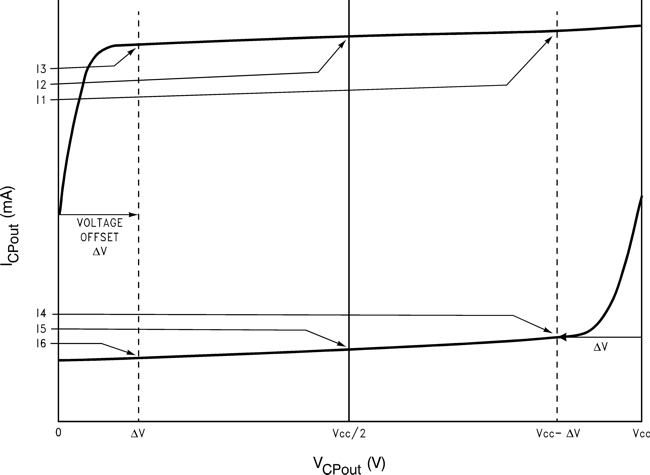
LMK04816 30179331.png Figure 4. Charge-Pump Current

I1 = Charge-Pump Sink Current at VCPout = VCC – ΔV

I2 = Charge-Pump Sink Current at VCPout = VCC / 2

I3 = Charge-Pump Sink Current at VCPout = ΔV

I4 = Charge-Pump Source Current at VCPout = VCC – ΔV

I5 = Charge-Pump Source Current at VCPout = VCC / 2

I6 = Charge-Pump Source Current at VCPout = ΔV

ΔV = Voltage offset from the positive and negative supply rails. Defined to be 0.5 V for this device.

7.1.1 Charge-Pump Output Current Magnitude Variation vs Charge-Pump Output Voltage

Use Equation 1 to calculate the charge-pump output current variation versus the charge-pump output voltage.
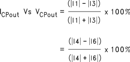
Equation 1. LMK04816 30179332.png

7.1.2 Charge-Pump Sink Current vs Charge-Pump Output Source Current Mismatch

Use Equation 2 to calculate the charge-pump sink current versus the source current mismatch.

Equation 2. LMK04816 30179333.png

7.1.3 Charge-Pump Output Current Magnitude Variation vs Temperature

Use Equation 3 to calculate the charge-pump output current magnitude variation versus the temperature.
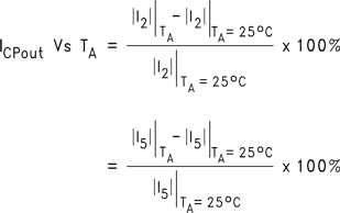
Equation 3. LMK04816 30179334.png

7.2 Differential Voltage Measurement Terminology

The differential voltage of a differential signal can be described by two different definitions causing confusion when reading data sheets or communicating with other engineers. This section addresses the measurement and description of a differential signal so that the reader can understand and discern between the two different definitions when used.

The first definition used to describe a differential signal is the absolute value of the voltage potential between the inverting and noninverting signal. The symbol for this first measurement is typically VID or VOD depending on if an input or output voltage is being described.

The second definition used to describe a differential signal is to measure the potential of the noninverting signal with respect to the inverting signal. The symbol for this second measurement is VSS and is a calculated parameter. Nowhere in the IC does this signal exist with respect to ground, it only exists in reference to its differential pair. VSS can be measured directly by oscilloscopes with floating references, otherwise this value can be calculated as twice the value of VOD as described in the first description.

Figure 5 shows the two different definitions side-by-side for inputs and Figure 6 shows the two different definitions side-by-side for outputs. The VID and VOD definitions show VA and VB DC levels that the noninverting and inverting signals toggle between with respect to ground. VSS input and output definitions show that if the inverting signal is considered the voltage potential reference, the noninverting signal voltage potential is now increasing and decreasing above and below the noninverting reference. Thus the peak-to-peak voltage of the differential signal can be measured.

VID and VOD are often defined as volts (V) and VSS is often defined as volts peak-to-peak (VPP).
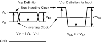
LMK04816 30179375.gif Figure 5. Two Different Definitions for Differential Input Signals
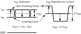
LMK04816 30179374.gif Figure 6. Two Different Definitions for Differential Output Signals

Refer to AN-912 Common Data Transmission Parameters and their Definitions (SNLA036) for more information.