ZHCSHN9A February 2018 – April 2018 LMK05028
PRODUCTION DATA.
- 1 特性
- 2 应用
- 3 说明
- 4 修订历史记录
- 5 说明 (续)
- 6 Pin Configuration and Functions
- 7 Specifications
- 8 Parameter Measurement Information
-
9 Detailed Description
- 9.1 Overview
- 9.2 Functional Block Diagrams
- 9.3
Feature Description
- 9.3.1 Oscillator Input (XO_P/N)
- 9.3.2 TCXO/OCXO Input (TCXO_IN)
- 9.3.3 Reference Inputs (INx_P/N)
- 9.3.4 Clock Input Interfacing and Termination
- 9.3.5 Reference Input Mux Selection
- 9.3.6 Hitless Switching
- 9.3.7 Gapped Clock Support on Reference Inputs
- 9.3.8 Input Clock and PLL Monitoring, Status, and Interrupts
- 9.3.9
PLL Channels
- 9.3.9.1 PLL Frequency Relationships
- 9.3.9.2 Analog PLL (APLL)
- 9.3.9.3 APLL XO Doubler
- 9.3.9.4 APLL Phase Frequency Detector (PFD) and Charge Pump
- 9.3.9.5 APLL Loop Filter
- 9.3.9.6 APLL Voltage Controlled Oscillator (VCO)
- 9.3.9.7 APLL VCO Post-Dividers (P1, P2)
- 9.3.9.8 APLL Fractional N Divider (N) With SDM
- 9.3.9.9 REF-DPLL Reference Divider (R)
- 9.3.9.10 TCXO/OCXO Input Doubler and M Divider
- 9.3.9.11 TCXO Mux
- 9.3.9.12 REF-DPLL and TCXO-DPLL Time-to-Digital Converter (TDC)
- 9.3.9.13 REF-DPLL and TCXO-DPLL Loop Filter
- 9.3.9.14 REF-DPLL and TCXO-DPLL Feedback Dividers
- 9.3.10 Output Clock Distribution
- 9.3.11 Output Channel Muxes
- 9.3.12 Output Dividers
- 9.3.13 Clock Outputs (OUTx_P/N)
- 9.3.14 Glitchless Output Clock Start-Up
- 9.3.15 Clock Output Interfacing and Termination
- 9.3.16 Output Synchronization (SYNC)
- 9.3.17 Zero-Delay Mode (ZDM) Configuration
- 9.3.18 PLL Cascading With Internal VCO Loopback
- 9.4 Device Functional Modes
- 9.5 Programming
- 9.6 Register Maps
- 10Application and Implementation
- 11Power Supply Recommendations
- 12Layout
- 13器件和文档支持
- 14机械、封装和可订购信息
9.3.15 Clock Output Interfacing and Termination
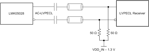
Figure 46 to Figure 50 show the recommended output interfacing and termination circuits. Unused clock outputs can be left floating and powered down by programming.

| Same applies for 1.8-V LVCMOS output to 1.8-V LVCMOS receiver. |
 Figure 47. AC-LVDS Output to LVDS Receiver With Internal Termination/Biasing
  Figure 48. AC-CML Output to CML Receiver With Internal Termination/Biasing
  Figure 49. AC-LVPECL Output to LVPECL Receiver With External Termination/Biasing
| If HCSL Internal Termination (50-Ω to GND) is enabled, replace 33-Ω with 0-Ω and remove 50-Ω external resistors. |