ZHCSHN9A February   2018  – April 2018 LMK05028

PRODUCTION DATA.  

  1. 特性
  2. 应用
  3. 说明
    1.     Device Images
      1.      简化方框图
  4. 修订历史记录
  5. 说明 (续)
  6. Pin Configuration and Functions
    1.     Pin Functions
    2. 6.1 Device Start-Up Modes
  7. Specifications
    1. 7.1 Absolute Maximum Ratings
    2. 7.2 ESD Ratings
    3. 7.3 Recommended Operating Conditions
    4. 7.4 Thermal Information
    5. 7.5 Electrical Characteristics
    6. 7.6 Timing Diagrams
    7. 7.7 Typical Characteristics
  8. Parameter Measurement Information
    1. 8.1 Output Clock Test Configurations
  9. Detailed Description
    1. 9.1 Overview
      1. 9.1.1 ITU-T G.8262 (SyncE) Standards Compliance
    2. 9.2 Functional Block Diagrams
      1. 9.2.1 PLL Architecture Overview
      2. 9.2.2 3-Loop Mode
        1. 9.2.2.1 PLL Output Clock Phase Noise Analysis in 3-Loop Mode
      3. 9.2.3 2-Loop REF-DPLL Mode
      4. 9.2.4 2-Loop TCXO-DPLL Mode
      5. 9.2.5 PLL Configurations for Common Applications
    3. 9.3 Feature Description
      1. 9.3.1  Oscillator Input (XO_P/N)
      2. 9.3.2  TCXO/OCXO Input (TCXO_IN)
      3. 9.3.3  Reference Inputs (INx_P/N)
      4. 9.3.4  Clock Input Interfacing and Termination
      5. 9.3.5  Reference Input Mux Selection
        1. 9.3.5.1 Automatic Input Selection
        2. 9.3.5.2 Manual Input Selection
      6. 9.3.6  Hitless Switching
      7. 9.3.7  Gapped Clock Support on Reference Inputs
      8. 9.3.8  Input Clock and PLL Monitoring, Status, and Interrupts
        1. 9.3.8.1 XO Input Monitoring
        2. 9.3.8.2 TCXO Input Monitoring
        3. 9.3.8.3 Reference Input Monitoring
          1. 9.3.8.3.1 Reference Validation Timer
          2. 9.3.8.3.2 Amplitude Monitor
          3. 9.3.8.3.3 Missing Pulse Monitor (Late Detect)
          4. 9.3.8.3.4 Runt Pulse Monitor (Early Detect)
          5. 9.3.8.3.5 Frequency Monitoring
          6. 9.3.8.3.6 Phase Valid Monitor for 1-PPS Inputs
        4. 9.3.8.4 PLL Lock Detectors
        5. 9.3.8.5 Tuning Word History
        6. 9.3.8.6 Status Outputs
        7. 9.3.8.7 Interrupt
      9. 9.3.9  PLL Channels
        1. 9.3.9.1  PLL Frequency Relationships
        2. 9.3.9.2  Analog PLL (APLL)
        3. 9.3.9.3  APLL XO Doubler
        4. 9.3.9.4  APLL Phase Frequency Detector (PFD) and Charge Pump
        5. 9.3.9.5  APLL Loop Filter
        6. 9.3.9.6  APLL Voltage Controlled Oscillator (VCO)
          1. 9.3.9.6.1 VCO Calibration
        7. 9.3.9.7  APLL VCO Post-Dividers (P1, P2)
        8. 9.3.9.8  APLL Fractional N Divider (N) With SDM
        9. 9.3.9.9  REF-DPLL Reference Divider (R)
        10. 9.3.9.10 TCXO/OCXO Input Doubler and M Divider
        11. 9.3.9.11 TCXO Mux
        12. 9.3.9.12 REF-DPLL and TCXO-DPLL Time-to-Digital Converter (TDC)
        13. 9.3.9.13 REF-DPLL and TCXO-DPLL Loop Filter
        14. 9.3.9.14 REF-DPLL and TCXO-DPLL Feedback Dividers
      10. 9.3.10 Output Clock Distribution
      11. 9.3.11 Output Channel Muxes
        1. 9.3.11.1 TCXO/Ref Bypass Mux
      12. 9.3.12 Output Dividers
      13. 9.3.13 Clock Outputs (OUTx_P/N)
        1. 9.3.13.1 AC-Differential Output (AC-DIFF)
        2. 9.3.13.2 HCSL Output
        3. 9.3.13.3 LVCMOS Output (1.8 V, 2.5 V)
        4. 9.3.13.4 Output Auto-Mute During LOL or LOS
      14. 9.3.14 Glitchless Output Clock Start-Up
      15. 9.3.15 Clock Output Interfacing and Termination
      16. 9.3.16 Output Synchronization (SYNC)
      17. 9.3.17 Zero-Delay Mode (ZDM) Configuration
      18. 9.3.18 PLL Cascading With Internal VCO Loopback
    4. 9.4 Device Functional Modes
      1. 9.4.1 Device Start-Up Modes
        1. 9.4.1.1 EEPROM Mode
        2. 9.4.1.2 ROM Mode
      2. 9.4.2 PLL Operating Modes
        1. 9.4.2.1 Free-Run Mode
        2. 9.4.2.2 Lock Acquisition
        3. 9.4.2.3 Locked Mode
        4. 9.4.2.4 Holdover Mode
      3. 9.4.3 PLL Start-Up Sequence
      4. 9.4.4 Digitally-Controlled Oscillator (DCO) Mode
        1. 9.4.4.1 DCO Frequency Step Size
        2. 9.4.4.2 DCO Direct-Write Mode
      5. 9.4.5 Zero-Delay Mode (ZDM)
      6. 9.4.6 Cascaded PLL Operation
    5. 9.5 Programming
      1. 9.5.1 Interface and Control
      2. 9.5.2 I2C Serial Interface
        1. 9.5.2.1 I2C Block Register Transfers
      3. 9.5.3 SPI Serial Interface
        1. 9.5.3.1 SPI Block Register Transfer
      4. 9.5.4 Register Map Generation
      5. 9.5.5 General Register Programming Sequence
      6. 9.5.6 EEPROM Programming Flow
        1. 9.5.6.1 EEPROM Programming Using Register Commit (Method #1)
          1. 9.5.6.1.1 Write SRAM Using Register Commit
          2. 9.5.6.1.2 Program EEPROM
        2. 9.5.6.2 EEPROM Programming Using Direct SRAM Writes (Method #2)
          1. 9.5.6.2.1 Write SRAM Using Direct Writes
      7. 9.5.7 Read SRAM
      8. 9.5.8 Read EEPROM
      9. 9.5.9 EEPROM Start-Up Mode Default Configuration
    6. 9.6 Register Maps
  10. 10Application and Implementation
    1. 10.1 Application Information
      1. 10.1.1 Device Start-Up Sequence
      2. 10.1.2 Power Down (PDN) Pin
      3. 10.1.3 Power Rail Sequencing, Power Supply Ramp Rate, and Mixing Supply Domains
        1. 10.1.3.1 Mixing Supplies
        2. 10.1.3.2 Power-On Reset (POR) Circuit
        3. 10.1.3.3 Powering Up From a Single-Supply Rail
        4. 10.1.3.4 Power Up From Split-Supply Rails
        5. 10.1.3.5 Non-Monotonic or Slow Power-Up Supply Ramp
      4. 10.1.4 Slow or Delayed XO Start-Up
    2. 10.2 Typical Application
      1. 10.2.1 Design Requirements
      2. 10.2.2 Detailed Design Procedure
      3. 10.2.3 Application Curves
    3. 10.3 Do's and Don'ts
  11. 11Power Supply Recommendations
    1. 11.1 Power Supply Bypassing
  12. 12Layout
    1. 12.1 Layout Guidelines
    2. 12.2 Layout Example
    3. 12.3 Thermal Reliability
  13. 13器件和文档支持
    1. 13.1 器件支持
      1. 13.1.1 时钟架构
      2. 13.1.2 TICS Pro
    2. 13.2 文档支持
      1. 13.2.1 相关文档
    3. 13.3 接收文档更新通知
    4. 13.4 社区资源
    5. 13.5 商标
    6. 13.6 静电放电警告
    7. 13.7 术语表
  14. 14机械、封装和可订购信息

封装选项

机械数据 (封装 | 引脚)
散热焊盘机械数据 (封装 | 引脚)
订购信息

PLL Cascading With Internal VCO Loopback

PLL cascading can be used when the second PLL (either PLL1 or PLL2) must be precisely locked to the frequency of the first PLL. The internal VCO loopback configuration options are implemented identically on both PLL channels, allowing PLL2 to be cascaded after PLL1 or vice versa. The internal VCO loopback clock from the first PLL can drive the REF-DPLL input path or the TCXO-DPLL input path if the TCXO loopback enable control is set. The second PLL can have reference validation enabled to qualify the VCO loopback clock from the first PLL stage to ensure that the second PLL stage has a stable and valid clock input from the first PLL stage before it acquires lock. The VCO loopback clock can be validated based on when the first PLL stage achieves frequency lock and/or phase lock on the REF-DPLL or frequency lock on the TCXO-DPLL. Once the VCO loopback clock is validated based on the enabled criteria, then the second PLL stage can begin to acquire lock. The VCO loopback dividers, loopback mux, and loopback reference validation options are programmable.

In the example shown in Figure 54, PLL2 is cascaded and locked to PLL1's internal VCO1 loopback clock through the two loopback dividers (fixed and programmable) and TCXO loopback muxes. PLL2 operates with a wide loop bandwidth to precisely track the DCO frequency adjustments applied to PLL1. This effectively applies DCO adjustments to both clock domains simultaneously, which would not be possible if both loops were operating in parallel (not cascaded) with separate DCO controls.
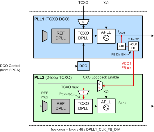
LMK05028 lmk05028-cascaded-pll-example-fbd.gifFigure 54. PLL Cascading Example With DCO Frequency Steering