ZHCSHN9A February   2018  – April 2018 LMK05028

PRODUCTION DATA.  

  1. 特性
  2. 应用
  3. 说明
    1.     Device Images
      1.      简化方框图
  4. 修订历史记录
  5. 说明 (续)
  6. Pin Configuration and Functions
    1.     Pin Functions
    2. 6.1 Device Start-Up Modes
  7. Specifications
    1. 7.1 Absolute Maximum Ratings
    2. 7.2 ESD Ratings
    3. 7.3 Recommended Operating Conditions
    4. 7.4 Thermal Information
    5. 7.5 Electrical Characteristics
    6. 7.6 Timing Diagrams
    7. 7.7 Typical Characteristics
  8. Parameter Measurement Information
    1. 8.1 Output Clock Test Configurations
  9. Detailed Description
    1. 9.1 Overview
      1. 9.1.1 ITU-T G.8262 (SyncE) Standards Compliance
    2. 9.2 Functional Block Diagrams
      1. 9.2.1 PLL Architecture Overview
      2. 9.2.2 3-Loop Mode
        1. 9.2.2.1 PLL Output Clock Phase Noise Analysis in 3-Loop Mode
      3. 9.2.3 2-Loop REF-DPLL Mode
      4. 9.2.4 2-Loop TCXO-DPLL Mode
      5. 9.2.5 PLL Configurations for Common Applications
    3. 9.3 Feature Description
      1. 9.3.1  Oscillator Input (XO_P/N)
      2. 9.3.2  TCXO/OCXO Input (TCXO_IN)
      3. 9.3.3  Reference Inputs (INx_P/N)
      4. 9.3.4  Clock Input Interfacing and Termination
      5. 9.3.5  Reference Input Mux Selection
        1. 9.3.5.1 Automatic Input Selection
        2. 9.3.5.2 Manual Input Selection
      6. 9.3.6  Hitless Switching
      7. 9.3.7  Gapped Clock Support on Reference Inputs
      8. 9.3.8  Input Clock and PLL Monitoring, Status, and Interrupts
        1. 9.3.8.1 XO Input Monitoring
        2. 9.3.8.2 TCXO Input Monitoring
        3. 9.3.8.3 Reference Input Monitoring
          1. 9.3.8.3.1 Reference Validation Timer
          2. 9.3.8.3.2 Amplitude Monitor
          3. 9.3.8.3.3 Missing Pulse Monitor (Late Detect)
          4. 9.3.8.3.4 Runt Pulse Monitor (Early Detect)
          5. 9.3.8.3.5 Frequency Monitoring
          6. 9.3.8.3.6 Phase Valid Monitor for 1-PPS Inputs
        4. 9.3.8.4 PLL Lock Detectors
        5. 9.3.8.5 Tuning Word History
        6. 9.3.8.6 Status Outputs
        7. 9.3.8.7 Interrupt
      9. 9.3.9  PLL Channels
        1. 9.3.9.1  PLL Frequency Relationships
        2. 9.3.9.2  Analog PLL (APLL)
        3. 9.3.9.3  APLL XO Doubler
        4. 9.3.9.4  APLL Phase Frequency Detector (PFD) and Charge Pump
        5. 9.3.9.5  APLL Loop Filter
        6. 9.3.9.6  APLL Voltage Controlled Oscillator (VCO)
          1. 9.3.9.6.1 VCO Calibration
        7. 9.3.9.7  APLL VCO Post-Dividers (P1, P2)
        8. 9.3.9.8  APLL Fractional N Divider (N) With SDM
        9. 9.3.9.9  REF-DPLL Reference Divider (R)
        10. 9.3.9.10 TCXO/OCXO Input Doubler and M Divider
        11. 9.3.9.11 TCXO Mux
        12. 9.3.9.12 REF-DPLL and TCXO-DPLL Time-to-Digital Converter (TDC)
        13. 9.3.9.13 REF-DPLL and TCXO-DPLL Loop Filter
        14. 9.3.9.14 REF-DPLL and TCXO-DPLL Feedback Dividers
      10. 9.3.10 Output Clock Distribution
      11. 9.3.11 Output Channel Muxes
        1. 9.3.11.1 TCXO/Ref Bypass Mux
      12. 9.3.12 Output Dividers
      13. 9.3.13 Clock Outputs (OUTx_P/N)
        1. 9.3.13.1 AC-Differential Output (AC-DIFF)
        2. 9.3.13.2 HCSL Output
        3. 9.3.13.3 LVCMOS Output (1.8 V, 2.5 V)
        4. 9.3.13.4 Output Auto-Mute During LOL or LOS
      14. 9.3.14 Glitchless Output Clock Start-Up
      15. 9.3.15 Clock Output Interfacing and Termination
      16. 9.3.16 Output Synchronization (SYNC)
      17. 9.3.17 Zero-Delay Mode (ZDM) Configuration
      18. 9.3.18 PLL Cascading With Internal VCO Loopback
    4. 9.4 Device Functional Modes
      1. 9.4.1 Device Start-Up Modes
        1. 9.4.1.1 EEPROM Mode
        2. 9.4.1.2 ROM Mode
      2. 9.4.2 PLL Operating Modes
        1. 9.4.2.1 Free-Run Mode
        2. 9.4.2.2 Lock Acquisition
        3. 9.4.2.3 Locked Mode
        4. 9.4.2.4 Holdover Mode
      3. 9.4.3 PLL Start-Up Sequence
      4. 9.4.4 Digitally-Controlled Oscillator (DCO) Mode
        1. 9.4.4.1 DCO Frequency Step Size
        2. 9.4.4.2 DCO Direct-Write Mode
      5. 9.4.5 Zero-Delay Mode (ZDM)
      6. 9.4.6 Cascaded PLL Operation
    5. 9.5 Programming
      1. 9.5.1 Interface and Control
      2. 9.5.2 I2C Serial Interface
        1. 9.5.2.1 I2C Block Register Transfers
      3. 9.5.3 SPI Serial Interface
        1. 9.5.3.1 SPI Block Register Transfer
      4. 9.5.4 Register Map Generation
      5. 9.5.5 General Register Programming Sequence
      6. 9.5.6 EEPROM Programming Flow
        1. 9.5.6.1 EEPROM Programming Using Register Commit (Method #1)
          1. 9.5.6.1.1 Write SRAM Using Register Commit
          2. 9.5.6.1.2 Program EEPROM
        2. 9.5.6.2 EEPROM Programming Using Direct SRAM Writes (Method #2)
          1. 9.5.6.2.1 Write SRAM Using Direct Writes
      7. 9.5.7 Read SRAM
      8. 9.5.8 Read EEPROM
      9. 9.5.9 EEPROM Start-Up Mode Default Configuration
    6. 9.6 Register Maps
  10. 10Application and Implementation
    1. 10.1 Application Information
      1. 10.1.1 Device Start-Up Sequence
      2. 10.1.2 Power Down (PDN) Pin
      3. 10.1.3 Power Rail Sequencing, Power Supply Ramp Rate, and Mixing Supply Domains
        1. 10.1.3.1 Mixing Supplies
        2. 10.1.3.2 Power-On Reset (POR) Circuit
        3. 10.1.3.3 Powering Up From a Single-Supply Rail
        4. 10.1.3.4 Power Up From Split-Supply Rails
        5. 10.1.3.5 Non-Monotonic or Slow Power-Up Supply Ramp
      4. 10.1.4 Slow or Delayed XO Start-Up
    2. 10.2 Typical Application
      1. 10.2.1 Design Requirements
      2. 10.2.2 Detailed Design Procedure
      3. 10.2.3 Application Curves
    3. 10.3 Do's and Don'ts
  11. 11Power Supply Recommendations
    1. 11.1 Power Supply Bypassing
  12. 12Layout
    1. 12.1 Layout Guidelines
    2. 12.2 Layout Example
    3. 12.3 Thermal Reliability
  13. 13器件和文档支持
    1. 13.1 器件支持
      1. 13.1.1 时钟架构
      2. 13.1.2 TICS Pro
    2. 13.2 文档支持
      1. 13.2.1 相关文档
    3. 13.3 接收文档更新通知
    4. 13.4 社区资源
    5. 13.5 商标
    6. 13.6 静电放电警告
    7. 13.7 术语表
  14. 14机械、封装和可订购信息

封装选项

机械数据 (封装 | 引脚)
散热焊盘机械数据 (封装 | 引脚)
订购信息

Interface and Control

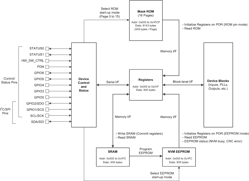
A system host device (MCU or FPGA) can use either I2C or SPI to access the register, SRAM, and EEPROM maps. The register and EEPROM map configurations are the same for I2C and SPI. The device can be initialized, controlled, and monitored through register access during normal operation (not hard reset by PDN = 0). Some device features can also be controlled and monitored through the external logic control and status pins.

In the absence of a host, the LMK05028 can self-start from its on-chip EEPROM or ROM page depending on the state of HW_SW_CTRL pin. The EEPROM or ROM page is used to initialize the registers upon device POR. The EEPROM configuration can be custom programmed through the register interface by either I2C or SPI. The ROM configurations are fixed in hardware and cannot be modified.

Figure 60 shows the device control pin, register, and memory interfaces. The arrows refer to the control interface directions between the different blocks.

The register map has 800 data bytes. Some registers (such as status, internal test/diagnostic bit fields) do not need to be written or accessed during device initialization.

The SRAM/EEPROM has one register page with 509 data bytes. The SRAM/EEPROM map has fewer bytes because not all bit fields are mapped from the register space. To program the EEPROM, it is necessary to write the register contents to SRAM (internal register commit or direct write), then Program EEPROM with the register contents from SRAM. The EEPROM cannot be written directly from the registers.

The ROM has sixteen register pages, and each page has 509 data bytes (same as EEPROM). The ROM contents are fixed in hardware and cannot be modified.
LMK05028 lmk05028_interface_control_block.gifFigure 60. Device Control, Register, and Memory Interfaces