ZHCSP13A september   2021  – june 2023 LMK1D1204P

PRODUCTION DATA  

  1.   1
  2. 特性
  3. 应用
  4. 说明
  5. Revision History
  6. Device Comparison
  7. Pin Configuration and Functions
  8. Specifications
    1. 7.1 Absolute Maximum Ratings
    2. 7.2 ESD Ratings
    3. 7.3 Recommended Operating Conditions
    4. 7.4 Thermal Information
    5. 7.5 Electrical Characteristics
    6. 7.6 Typical Characteristics
  9. Parameter Measurement Information
  10. Detailed Description
    1. 9.1 Overview
    2. 9.2 Functional Block Diagram
    3. 9.3 Feature Description
      1. 9.3.1 Fail-Safe Input
    4. 9.4 Device Functional Modes
      1. 9.4.1 LVDS Output Termination
      2. 9.4.2 Input Termination
  11. 10Application and Implementation
    1. 10.1 Application Information
    2. 10.2 Typical Application
      1. 10.2.1 Design Requirements
      2. 10.2.2 Detailed Design Procedure
      3. 10.2.3 Application Curves
    3. 10.3 Power Supply Recommendations
    4. 10.4 Layout
      1. 10.4.1 Layout Guidelines
      2. 10.4.2 Layout Examples
  12. 11Device and Documentation Support
    1. 11.1 Documentation Support
      1. 11.1.1 Related Documentation
    2. 11.2 支持资源
    3. 11.3 Trademarks
    4. 11.4 静电放电警告
    5. 11.5 术语表
  13. 12Mechanical, Packaging, and Orderable Information

封装选项

机械数据 (封装 | 引脚)
散热焊盘机械数据 (封装 | 引脚)
订购信息

Application Curves

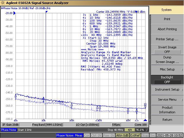
This section shows the low additive noise for the LMK1D1204P. The low noise 156.25-MHz source with 24-fs RMS jitter shown in Figure 10-2 drives the LMK1D1204P, resulting in 46.4-fs RMS when integrated from 12 kHz to 20 MHz (see Figure 10-3). The resultant additive jitter is 39.7-fs RMS for this configuration.
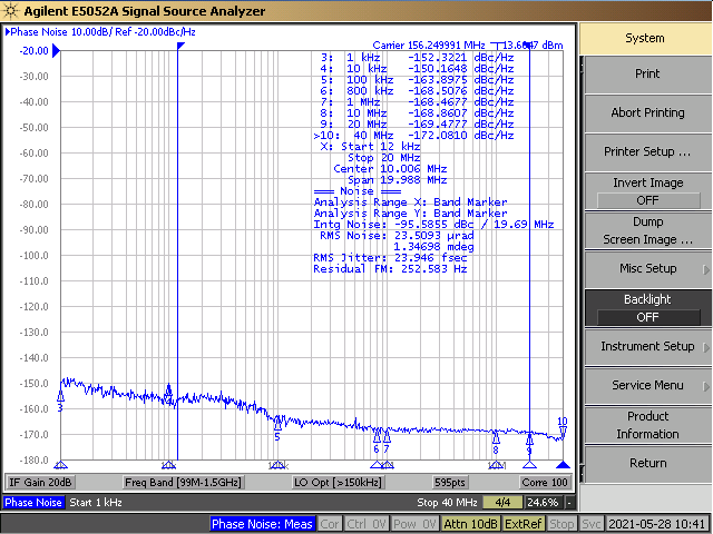
GUID-20210602-CA0I-GN5T-HMCW-60MTDBQFQ7DL-low.png
Note: Reference signal is a low-noise Rhode and Schwarz SMA100B
Figure 10-2 LMK1D1204P Reference Phase Noise, 156.25 MHz, 24-fs RMS (12 kHz to 20 MHz)
GUID-20210602-CA0I-J5LV-QK4Z-LNRFSWZ0SS7C-low.pngFigure 10-3 LMK1D1204P Output Phase Noise, 156.25 MHz, 46.4-fs RMS (12 kHz to 20 MHz)