ZHCSP66A october   2021  – april 2023 LMK1D1212 , LMK1D1216

PRODUCTION DATA  

  1. 特性
  2. 应用
  3. 说明
  4. Revision History
  5. Device Comparison Table
  6. Pin Configuration and Functions
  7. Specifications
    1. 7.1 Absolute Maximum Ratings
    2. 7.2 ESD Ratings
    3. 7.3 Recommended Operating Conditions
    4. 7.4 Thermal Information
    5. 7.5 Electrical Characteristics
    6. 7.6 Typical Characteristics
  8. Parameter Measurement Information
  9. Detailed Description
    1. 9.1 Overview
    2. 9.2 Functional Block Diagram
    3. 9.3 Feature Description
      1. 9.3.1 Fail-Safe Input and Hysteresis
      2. 9.3.2 Input Mux
    4. 9.4 Device Functional Modes
      1. 9.4.1 LVDS Output Termination
      2. 9.4.2 Input Termination
  10. 10Application and Implementation
    1. 10.1 Application Information
    2. 10.2 Typical Application
      1. 10.2.1 Design Requirements
      2. 10.2.2 Detailed Design Procedure
      3. 10.2.3 Application Curves
    3. 10.3 Power Supply Recommendations
    4. 10.4 Layout
      1. 10.4.1 Layout Guidelines
      2. 10.4.2 Layout Examples
  11. 11Device and Documentation Support
    1. 11.1 Documentation Support
      1. 11.1.1 Related Documentation
    2. 11.2 接收文档更新通知
    3. 11.3 支持资源
    4. 11.4 Trademarks
    5. 11.5 静电放电警告
    6. 11.6 术语表
  12. 12Mechanical, Packaging, and Orderable Information

封装选项

机械数据 (封装 | 引脚)
散热焊盘机械数据 (封装 | 引脚)
订购信息

Input Termination

The LMK1D121x inputs can be interfaced with LVDS, LVPECL, LP-HCSL, HCSL, CML, or LVCMOS drivers.

LVDS drivers can be connected to LMK1D121x inputs with DC and AC coupling as shown Figure 9-3 and Figure 9-4, respectively.

GUID-26D1BA4C-15C6-4EDE-986C-9BA718A3F8F4-low.gifFigure 9-3 LVDS Clock Driver Connected to LMK1D121x Input (DC-Coupled)
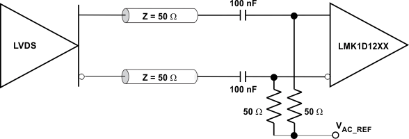
GUID-D414B416-8EEF-4FD3-9FF4-D0181EEAAE50-low.gifFigure 9-4 LVDS Clock Driver Connected to LMK1D121x Input (AC-Coupled)

Figure 9-5 shows how to connect LVPECL inputs to the LMK1D121x. The series resistors are required to reduce the LVPECL signal swing if the signal swing is >1.6 VPP.
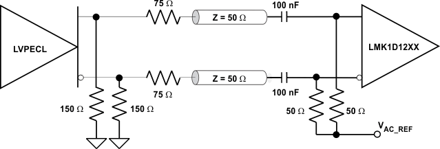
GUID-0B5C5867-84DA-4D75-8A32-80206BF55FE9-low.gifFigure 9-5 LVPECL Clock Driver Connected to LMK1D121x Input

Figure 9-6 shows how to couple a LVCMOS clock input to the LMK1D121x directly.
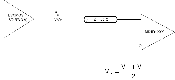
GUID-A4438E7E-6368-4CD7-A79C-9D153F0B9A2C-low.gifFigure 9-6 1.8-V, 2.5-V, or 3.3-V LVCMOS Clock Driver Connected to LMK1D121x Input

For unused input, TI recommends grounding both input pins (INP, INN) using 1-kΩ resistors.