ZHCSOY4B september   2021  – june 2023 LMK1D2102 , LMK1D2104

PRODUCTION DATA  

  1.   1
  2. 特性
  3. 应用
  4. 说明
  5. Revision History
  6. Device Comparison
  7. Pin Configuration and Functions
  8. Specifications
    1. 7.1 Absolute Maximum Ratings
    2. 7.2 ESD Ratings
    3. 7.3 Recommended Operating Conditions
    4. 7.4 Thermal Information
    5. 7.5 Electrical Characteristics
    6. 7.6 Typical Characteristics
  9. Parameter Measurement Information
  10. Detailed Description
    1. 9.1 Overview
    2. 9.2 Functional Block Diagram
    3. 9.3 Feature Description
      1. 9.3.1 Fail-Safe Inputs
    4. 9.4 Device Functional Modes
      1. 9.4.1 LVDS Output Termination
      2. 9.4.2 Input Termination
  11. 10Application and Implementation
    1. 10.1 Application Information
    2. 10.2 Typical Application
      1. 10.2.1 Design Requirements
      2. 10.2.2 Detailed Design Procedure
      3. 10.2.3 Application Curves
    3. 10.3 Power Supply Recommendations
    4. 10.4 Layout
      1. 10.4.1 Layout Guidelines
      2. 10.4.2 Layout Example
  12. 11Device and Documentation Support
    1. 11.1 Documentation Support
      1. 11.1.1 Related Documentation
    2. 11.2 接收文档更新通知
    3. 11.3 支持资源
    4. 11.4 Trademarks
    5. 11.5 静电放电警告
    6. 11.6 术语表
  13. 12Mechanical, Packaging, and Orderable Information

封装选项

机械数据 (封装 | 引脚)
散热焊盘机械数据 (封装 | 引脚)
订购信息

Input Termination

The LMK1D210x inputs can be interfaced with LVDS, LVPECL, HCSL or LVCMOS drivers.

LVDS drivers can be connected to LMK1D210x inputs with DC- and AC-coupling as shown Figure 9-3 and Figure 9-4 (respectively).

GUID-AD5A5C40-DB86-4529-A154-34FAF615A955-low.gifFigure 9-3 LVDS Clock Driver Connected to LMK1D210x Input (DC-Coupled)
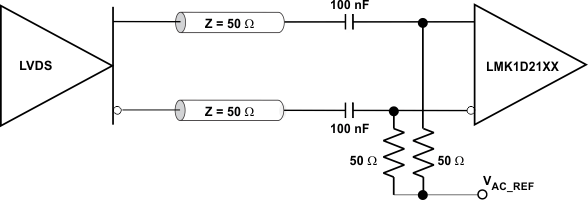
GUID-C81AE221-5619-4A29-A553-293ABB5AC66F-low.gifFigure 9-4 LVDS Clock Driver Connected to LMK1D210x Input (AC-Coupled)

Figure 9-5 shows how to connect LVPECL inputs to the LMK1D210x. The series resistors are required to reduce the LVPECL signal swing if the signal swing is >1.6 VPP.
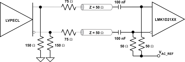
GUID-3C5139B1-50DB-4761-883E-1ED500F14AE5-low.gifFigure 9-5 LVPECL Clock Driver Connected to LMK1D210x Input

Figure 9-6 illustrates how to couple a LVCMOS clock input to the LMK1D210x directly.

GUID-20210518-CA0I-DKRD-D0KN-Z6DTT2Q5MVJB-low.svg Figure 9-6 1.8-V/2.5-V/3.3-V LVCMOS Clock Driver Connected to LMK1D210x Input

Unused inputs can be left floating thus reducing the need for additional components.