ZHCSLM0A May   2020  – January 2021 LMK5B12204

PRODUCTION DATA  

  1. 特性
  2. 应用
  3. 说明
  4. Revision History
  5. 说明(续)
  6. Pin Configuration and Functions
    1. 6.1 Device Start-Up Modes
  7. Specifications
    1. 7.1 Absolute Maximum Ratings
    2. 7.2 ESD Ratings
    3. 7.3 Recommended Operating Conditions
    4. 7.4 Thermal Information: 4-Layer JEDEC Standard PCB
    5. 7.5 Thermal Information: 10-Layer Custom PCB
    6. 7.6 Electrical Characteristics
    7. 7.7 Timing Diagrams
    8. 7.8 Typical Characteristics
  8. Parameter Measurement Information
    1. 8.1 Output Clock Test Configurations
  9. Detailed Description
    1. 9.1 Overview
      1. 9.1.1 ITU-T G.8262 (SyncE) Standards Compliance
    2. 9.2 Functional Block Diagram
      1. 9.2.1 PLL Architecture Overview
      2. 9.2.2 DPLL Mode
      3. 9.2.3 APLL-Only Mode
    3. 9.3 Feature Description
      1. 9.3.1  Oscillator Input (XO_P/N)
      2. 9.3.2  Reference Inputs (PRIREF_P/N and SECREF_P/N)
        1. 9.3.2.1 Programmable Input Hysteresis
      3. 9.3.3  Clock Input Interfacing and Termination
      4. 9.3.4  Reference Input Mux Selection
        1. 9.3.4.1 Automatic Input Selection
        2. 9.3.4.2 Manual Input Selection
      5. 9.3.5  Hitless Switching
        1. 9.3.5.1 Hitless Switching With 1-PPS Inputs
      6. 9.3.6  Gapped Clock Support on Reference Inputs
      7. 9.3.7  Input Clock and PLL Monitoring, Status, and Interrupts
        1. 9.3.7.1 XO Input Monitoring
        2. 9.3.7.2 Reference Input Monitoring
          1. 9.3.7.2.1 Reference Validation Timer
          2. 9.3.7.2.2 Amplitude Monitor
          3. 9.3.7.2.3 Frequency Monitoring
          4. 9.3.7.2.4 Missing Pulse Monitor (Late Detect)
          5. 9.3.7.2.5 Runt Pulse Monitor (Early Detect)
          6. 9.3.7.2.6 Phase Valid Monitor for 1-PPS Inputs
        3. 9.3.7.3 PLL Lock Detectors
        4. 9.3.7.4 Tuning Word History
        5. 9.3.7.5 Status Outputs
        6. 9.3.7.6 Interrupt
      8. 9.3.8  PLL Relationships
        1. 9.3.8.1  PLL Frequency Relationships
        2. 9.3.8.2  Analog PLLs (APLL1, APLL2)
        3. 9.3.8.3  APLL Reference Paths
          1. 9.3.8.3.1 APLL XO Doubler
          2. 9.3.8.3.2 APLL1 XO Reference (R) Divider
          3. 9.3.8.3.3 APLL2 Reference (R) Dividers
        4. 9.3.8.4  APLL Phase Frequency Detector (PFD) and Charge Pump
        5. 9.3.8.5  APLL Feedback Divider Paths
          1. 9.3.8.5.1 APLL1 N Divider With SDM
          2. 9.3.8.5.2 APLL2 N Divider With SDM
        6. 9.3.8.6  APLL Loop Filters (LF1, LF2)
        7. 9.3.8.7  APLL Voltage Controlled Oscillators (VCO1, VCO2)
          1. 9.3.8.7.1 VCO Calibration
        8. 9.3.8.8  APLL VCO Clock Distribution Paths (P1, P2)
        9. 9.3.8.9  DPLL Reference (R) Divider Paths
        10. 9.3.8.10 DPLL Time-to-Digital Converter (TDC)
        11. 9.3.8.11 DPLL Loop Filter (DLF)
        12. 9.3.8.12 DPLL Feedback (FB) Divider Path
      9. 9.3.9  Output Clock Distribution
      10. 9.3.10 Output Channel Muxes
      11. 9.3.11 Output Dividers (OD)
      12. 9.3.12 Clock Outputs (OUTx_P/N)
        1. 9.3.12.1 AC-Differential Output (AC-DIFF)
        2. 9.3.12.2 HCSL Output
        3. 9.3.12.3 1.8-V LVCMOS Output
        4. 9.3.12.4 Output Auto-Mute During LOL
      13. 9.3.13 Glitchless Output Clock Start-Up
      14. 9.3.14 Clock Output Interfacing and Termination
      15. 9.3.15 Output Synchronization (SYNC)
    4. 9.4 Device Functional Modes
      1. 9.4.1 Device Start-Up Modes
        1. 9.4.1.1 EEPROM Mode
        2. 9.4.1.2 ROM Mode
      2. 9.4.2 PLL Operating Modes
        1. 9.4.2.1 Free-Run Mode
        2. 9.4.2.2 Lock Acquisition
        3. 9.4.2.3 Locked Mode
        4. 9.4.2.4 Holdover Mode
      3. 9.4.3 PLL Start-Up Sequence
      4. 9.4.4 Digitally-Controlled Oscillator (DCO) Mode
        1. 9.4.4.1 DCO Frequency Step Size
        2. 9.4.4.2 DCO Direct-Write Mode
    5. 9.5 Programming
      1. 9.5.1 Interface and Control
      2. 9.5.2 I2C Serial Interface
        1. 9.5.2.1 I2C Block Register Transfers
      3. 9.5.3 SPI Serial Interface
        1. 9.5.3.1 SPI Block Register Transfer
      4. 9.5.4 Register Map and EEPROM Map Generation
      5. 9.5.5 General Register Programming Sequence
      6. 9.5.6 EEPROM Programming Flow
        1. 9.5.6.1 EEPROM Programming Using Method #1 (Register Commit)
          1. 9.5.6.1.1 Write SRAM Using Register Commit
          2. 9.5.6.1.2 Program EEPROM
        2. 9.5.6.2 EEPROM Programming Using Method #2 (Direct Writes)
          1. 9.5.6.2.1 Write SRAM Using Direct Writes
          2. 9.5.6.2.2 User-Programmable Fields In EEPROM
      7. 9.5.7 Read SRAM
      8. 9.5.8 Read EEPROM
      9. 9.5.9 EEPROM Start-Up Mode Default Configuration
  10. 10Application and Implementation
    1. 10.1 Application Information
      1. 10.1.1 Device Start-Up Sequence
      2. 10.1.2 Power Down (PDN) Pin
      3. 10.1.3 Power Rail Sequencing, Power Supply Ramp Rate, and Mixing Supply Domains
        1. 10.1.3.1 Mixing Supplies
        2. 10.1.3.2 Power-On Reset (POR) Circuit
        3. 10.1.3.3 Powering Up From a Single-Supply Rail
        4. 10.1.3.4 Power Up From Split-Supply Rails
        5. 10.1.3.5 Non-Monotonic or Slow Power-Up Supply Ramp
      4. 10.1.4 Slow or Delayed XO Start-Up
    2. 10.2 Typical Application
      1. 10.2.1 Design Requirements
      2. 10.2.2 Detailed Design Procedure
      3. 10.2.3 Application Curves
    3. 10.3 Do's and Don'ts
  11. 11Power Supply Recommendations
    1. 11.1 Power Supply Bypassing
    2. 11.2 Device Current and Power Consumption
      1. 11.2.1 Current Consumption Calculations
      2. 11.2.2 Power Consumption Calculations
      3. 11.2.3 Example
  12. 12Layout
    1. 12.1 Layout Guidelines
    2. 12.2 Layout Example
    3. 12.3 Thermal Reliability
      1. 12.3.1 Support for PCB Temperature up to 105 °C
  13. 13Device and Documentation Support
    1. 13.1 Device Support
      1. 13.1.1 TICS Pro
      2. 13.1.2 Related Documentation
    2. 13.2 接收文档更新通知
    3. 13.3 支持资源
    4. 13.4 Trademarks
    5. 13.5 静电放电警告
    6. 13.6 术语表
  14. 14Mechanical, Packaging, and Orderable Information
    1. 14.1 Package Option Addendum
      1. 14.1.1 Packaging Information
      2. 14.1.2 Tape and Reel Information

封装选项

机械数据 (封装 | 引脚)
散热焊盘机械数据 (封装 | 引脚)
订购信息

Oscillator Input (XO_P/N)

The XO input is the reference clock for the fractional-N APLLs. The XO input determines the output frequency accuracy and stability in free-run or holdover modes.

For DPLL mode, the XO frequency must have a non-integer relationship with the VCO1 frequency so APLL1 can operate in fractional mode. For APLL-only mode, the XO frequency can have an integer or fractional relationship with the VCO1 and/or VCO2 frequencies.

In DPLL mode applications, such as SyncE and IEEE 1588, the XO input can be driven by a low-frequency TCXO, OCXO, or external traceable clock that conforms to the frequency accuracy and holdover stability required by the applicable synchronization standard. TCXO and OCXO frequencies of 12.8, 19.2, 19.44, 24, 24.576, and 30.72 MHz are commonly available and cost-effective options that allow the APLL1 to operate in fractional mode for a VCO1 frequency of 2.5 GHz.

An XO/TCXO/OCXO source with low-frequency or a high-phase jitter/noise floor will have no impact on the output jitter performance because the BAW VCO determines the jitter and phase noise over the 12-kHz to 20-MHz integration bandwidth.

The XO input buffer has programmable input on-chip termination and AC-coupled input biasing configurations as shown in Figure 9-6. The buffered XO path also drives the input monitoring blocks.
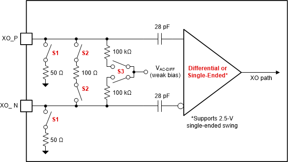
GUID-6E084E86-E8DF-4BA0-830D-381A44750EAB-low.gifFigure 9-6 XO Input Buffer

Table 9-1 lists the typical XO input buffer configurations for common clock interface types.

Table 9-1 XO Input Buffer Modes
XO_TYPEINPUT TYPESINTERNAL SWITCH SETTINGS
INTERNAL TERM. (S1, S2)(1)INTERNAL BIAS (S3)(2)
1hDifferential
(DC-coupled or AC-coupled)
OFFON (1.3 V)
3hDifferential
(AC-coupled or DC-coupled, Internal 100-Ω)
100 ΩON (1.3 V)
4hHCSL
(DC-coupled, internal 50-Ω)
50 ΩOFF
8hLVCMOS
(DC-coupled)
OFFOFF
ChSingle-ended
(DC-coupled, internal 50-Ω)
50 ΩOFF
S1, S2: OFF = External termination is assumed.
S3: OFF = External input bias or DC coupling is assumed.