ZHCSLT9B March   2022  – July 2022 LMK5B33216

PRODUCTION DATA  

  1. 特性
  2. 应用
  3. 说明
  4. Revision History
  5. Pin Configuration and Functions
  6. Specifications
    1. 6.1 Absolute Maximum Ratings
    2. 6.2 ESD Ratings
    3. 6.3 Recommended Operating Conditions
    4. 6.4 Thermal Information
    5. 6.5 Electrical Characteristics
    6. 6.6 Timing Diagrams
    7. 6.7 Typical Characteristics
  7. Parameter Measurement Information
    1. 7.1 Differential Voltage Measurement Terminology
    2. 7.2 Output Clock Test Configurations
  8. Detailed Description
    1. 8.1 Overview
    2. 8.2 Functional Block Diagram
      1. 8.2.1 PLL Architecture Overview
      2. 8.2.2 DPLL
        1. 8.2.2.1 Independent DPLL Operation
        2. 8.2.2.2 Cascaded DPLL Operation
        3. 8.2.2.3 APLL Cascaded With DPLL
      3. 8.2.3 APLL-Only Mode
    3. 8.3 Feature Description
      1. 8.3.1  Oscillator Input (XO)
      2. 8.3.2  Reference Inputs
      3. 8.3.3  Clock Input Interfacing and Termination
      4. 8.3.4  Reference Input Mux Selection
        1. 8.3.4.1 Automatic Input Selection
        2. 8.3.4.2 Manual Input Selection
      5. 8.3.5  Hitless Switching
        1. 8.3.5.1 Hitless Switching With Phase Cancellation
        2. 8.3.5.2 Hitless Switching With Phase Slew Control
        3. 8.3.5.3 Hitless Switching With 1-PPS Inputs
      6. 8.3.6  Gapped Clock Support on Reference Inputs
      7. 8.3.7  Input Clock and PLL Monitoring, Status, and Interrupts
        1. 8.3.7.1 XO Input Monitoring
        2. 8.3.7.2 Reference Input Monitoring
          1. 8.3.7.2.1 Reference Validation Timer
          2. 8.3.7.2.2 Frequency Monitoring
          3. 8.3.7.2.3 Missing Pulse Monitor (Late Detect)
          4. 8.3.7.2.4 Runt Pulse Monitor (Early Detect)
          5. 8.3.7.2.5 Phase Valid Monitor for 1-PPS Inputs
        3. 8.3.7.3 PLL Lock Detectors
        4. 8.3.7.4 Tuning Word History
        5. 8.3.7.5 Status Outputs
        6. 8.3.7.6 Interrupt
      8. 8.3.8  PLL Relationships
        1. 8.3.8.1  PLL Frequency Relationships
          1. 8.3.8.1.1 APLL Phase Detector Frequency
          2. 8.3.8.1.2 APLL VCO Frequency
          3. 8.3.8.1.3 DPLL TDC Frequency
          4. 8.3.8.1.4 DPLL VCO Frequency
          5. 8.3.8.1.5 Clock Output Frequency
        2. 8.3.8.2  Analog PLLs (APLL1, APLL2, APLL3)
        3. 8.3.8.3  APLL Reference Paths
          1. 8.3.8.3.1 APLL XO Doubler
          2. 8.3.8.3.2 APLL XO Reference (R) Divider
        4. 8.3.8.4  APLL Phase Frequency Detector (PFD) and Charge Pump
        5. 8.3.8.5  APLL Feedback Divider Paths
          1. 8.3.8.5.1 APLL N Divider With SDM
        6. 8.3.8.6  APLL Loop Filters (LF1, LF2, LF3)
        7. 8.3.8.7  APLL Voltage-Controlled Oscillators (VCO1, VCO2, VCO3)
          1. 8.3.8.7.1 VCO Calibration
        8. 8.3.8.8  APLL VCO Clock Distribution Paths
        9. 8.3.8.9  DPLL Reference (R) Divider Paths
        10. 8.3.8.10 DPLL Time-to-Digital Converter (TDC)
        11. 8.3.8.11 DPLL Loop Filter (DLF)
        12. 8.3.8.12 DPLL Feedback (FB) Divider Path
      9. 8.3.9  Output Clock Distribution
      10. 8.3.10 Output Channel Muxes
      11. 8.3.11 Output Dividers (OD)
      12. 8.3.12 SYSREF/1PPS
      13. 8.3.13 Output Delay
      14. 8.3.14 Clock Outputs (OUTx_P/N)
        1. 8.3.14.1 Differential Output
        2. 8.3.14.2 LVCMOS Output
        3. 8.3.14.3 SYSREF/1PPS Output Replication
        4. 8.3.14.4 Output Auto-Mute During LOL
      15. 8.3.15 Glitchless Output Clock Start-Up
      16. 8.3.16 Clock Output Interfacing and Termination
      17. 8.3.17 Output Synchronization (SYNC)
      18. 8.3.18 Zero-Delay Mode (ZDM) Synchronization
      19. 8.3.19 Time Elapsed Counter (TEC)
        1. 8.3.19.1 Configuring TEC Functionality
        2. 8.3.19.2 SPI as a Trigger Source
        3. 8.3.19.3 GPIO Pin as a TEC Trigger Source
          1. 8.3.19.3.1 An Example: Making a Time Elapsed Measurement Using TEC and GPIO1 as Trigger
        4. 8.3.19.4 TEC Timing
        5. 8.3.19.5 Other TEC Behavior
    4. 8.4 Device Functional Modes
      1. 8.4.1 Device Start-Up
        1. 8.4.1.1 ROM Selection
        2. 8.4.1.2 EEPROM Overlay
      2. 8.4.2 DPLL Operating States
        1. 8.4.2.1 Free-Run
        2. 8.4.2.2 Lock Acquisition
        3. 8.4.2.3 DPLL Locked
        4. 8.4.2.4 Holdover
      3. 8.4.3 PLL Start-Up Sequence
      4. 8.4.4 Digitally-Controlled Oscillator (DCO) Frequency and Phase Adjustment
        1. 8.4.4.1 DPLL DCO Control
          1. 8.4.4.1.1 DPLL DCO Relative Adjustment Frequency Step Size
          2. 8.4.4.1.2 APLL DCO Frequency Step Size
      5. 8.4.5 APLL Frequency Control
      6. 8.4.6 Zero-Delay Mode Synchronization
    5. 8.5 Programming
      1. 8.5.1 Interface and Control
      2. 8.5.2 I2C Serial Interface
        1. 8.5.2.1 I2C Block Register Transfers
      3. 8.5.3 SPI Serial Interface
        1. 8.5.3.1 SPI Block Register Transfer
      4. 8.5.4 Register Map Generation
      5. 8.5.5 General Register Programming Sequence
  9. Application and Implementation
    1. 9.1 Application Information
      1. 9.1.1 Device Start-Up Sequence
      2. 9.1.2 Power Down (PD#) Pin
      3. 9.1.3 Strap Pins for Start-Up
      4. 9.1.4 Pin States
      5. 9.1.5 ROM and EEPROM
      6. 9.1.6 Power Rail Sequencing, Power Supply Ramp Rate, and Mixing Supply Domains
        1. 9.1.6.1 Power-On Reset (POR) Circuit
        2. 9.1.6.2 Powering Up From a Single-Supply Rail
        3. 9.1.6.3 Power Up From Split-Supply Rails
        4. 9.1.6.4 Non-Monotonic or Slow Power-Up Supply Ramp
      7. 9.1.7 Slow or Delayed XO Start-Up
    2. 9.2 Typical Application
      1. 9.2.1 Design Requirements
      2. 9.2.2 Detailed Design Procedure
      3. 9.2.3 Application Curves
    3. 9.3 Do's and Don'ts
    4. 9.4 Power Supply Recommendations
      1. 9.4.1 Power Supply Bypassing
    5. 9.5 Layout
      1. 9.5.1 Layout Guidelines
      2. 9.5.2 Layout Example
      3. 9.5.3 Thermal Reliability
  10. 10Device and Documentation Support
    1. 10.1 Device Support
      1. 10.1.1 Development Support
        1. 10.1.1.1 Clock Tree Architect Programming Software
        2. 10.1.1.2 Texas Instruments Clocks and Synthesizers (TICS) Pro Software
        3. 10.1.1.3 PLLatinum™ Simulation Tool
    2. 10.2 Documentation Support
      1. 10.2.1 Related Documentation
    3. 10.3 接收文档更新通知
    4. 10.4 支持资源
    5. 10.5 Trademarks
    6. 10.6 术语表
    7. 10.7 静电放电警告
  11. 11Mechanical, Packaging, and Orderable Information

封装选项

机械数据 (封装 | 引脚)
散热焊盘机械数据 (封装 | 引脚)
订购信息

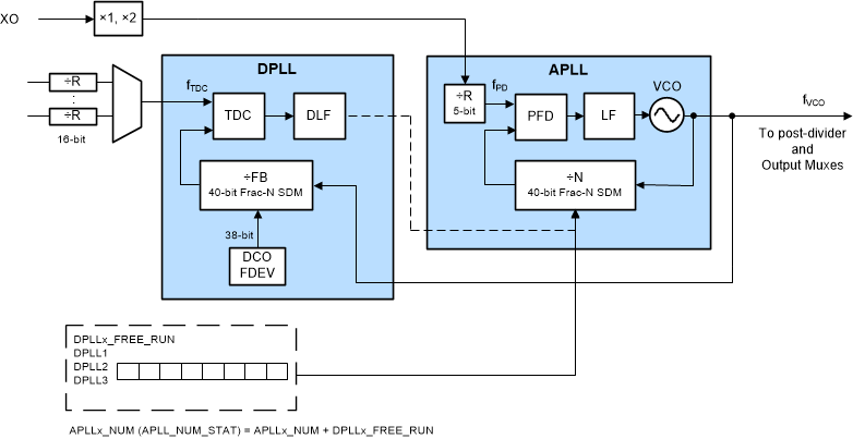
APLL Frequency Control

The device can also support APLL frequency and phase control through writing the 40-bit register DPLLx_FREE_RUN[39:0] while the DPLL is in holdover or not used. If the reference clock in a free-run mode or disabled, DPLL will disconnect with APLL, but users can still adjust frequency and phase accuracy.

To enable APLL DCO control, set DPLLx_LOOP_EN = 1, and PLLx_MODE = 1 for 40-bit fractional denominator. DPLLx_EN may be set = 0.

GUID-05D650D4-E792-4CFA-AAF8-CF4A957A0306-low.gif
Figure 8-39 APLL DCO Mode

There are two alternative methods in adjusting the APLL DCO.

  • Absolute frequency adjustment
    • Set DPLLx_HIST_EN = 0
    • Effective APLLx_NUM (APLLx_NUM_STAT) = APLLx_NUM + DPLLx_FREE_RUN
      • The APLLx_NUM_STAT is a read-only register and can be read back.
      • The DPLL loop filter block will modify the APLLx_NUM_STAT based on DPLLx_FREE_RUN value.
    • DPLLx_FREE_RUN is a 40-bit 2s complement number
  • Relative frequency adjustment
    • Set DPLLx_HIST_EN = 1
    • DPLLx_FREE_RUN value is fed into the APLLx_NUM at a controlled rate defined by a step size register and step period register.
    • If another DPLLx_FREE_RUN write occurs before the LMK is complete in making the last adjustment, any remaining steps are lost and the new value begins to feed the APLL numerator.
    • A flag is set when the DPLLx_FREE_RUN word is fully fed into the effective APLLx_NUM (APLL_NUM_STAT).