ZHCSMJ6B
November 2020 – March 2021
LMK5C33216
PRODUCTION DATA
1
特性
2
应用
3
说明
4
Revision History
5
Device Comparison
6
Pin Configuration and Functions
7
Specifications
7.1
Absolute Maximum Ratings
7.2
ESD Ratings
7.3
Recommended Operating Conditions
7.4
Thermal Information
7.5
Electrical Characteristics
7.6
Timing Diagrams
8
Parameter Measurement Information
8.1
Differential Voltage Measurement Terminology
8.2
Output Clock Test Configurations
9
Detailed Description
9.1
Overview
9.2
Functional Block Diagram
9.2.1
PLL Architecture Overview
9.2.2
DPLL
9.2.2.1
Independent DPLL Operation
9.2.2.2
Cascaded DPLL Operation
9.2.2.3
APLL Cascaded with DPLL
9.2.3
APLL-Only Mode
9.3
Feature Description
9.3.1
Oscillator Input (XO)
9.3.2
Reference Inputs
9.3.3
Clock Input Interfacing and Termination
9.3.4
Reference Input Mux Selection
9.3.4.1
Automatic Input Selection
9.3.4.2
Manual Input Selection
9.3.5
Hitless Switching
9.3.5.1
Hitless Switching with Phase Cancellation
9.3.5.2
Hitless Switching With Phase Slew Control
9.3.5.3
Hitless Switching With 1-PPS Inputs
9.3.6
Gapped Clock Support on Reference Inputs
9.3.7
Input Clock and PLL Monitoring, Status, and Interrupts
9.3.7.1
XO Input Monitoring
9.3.7.2
Reference Input Monitoring
9.3.7.2.1
Reference Validation Timer
9.3.7.2.2
Frequency Monitoring
9.3.7.2.3
Missing Pulse Monitor (Late Detect)
9.3.7.2.4
Runt Pulse Monitor (Early Detect)
9.3.7.2.5
Phase Valid Monitor for 1-PPS Inputs
9.3.7.3
PLL Lock Detectors
9.3.7.4
Tuning Word History
9.3.7.5
Status Outputs
9.3.7.6
Interrupt
9.3.8
PLL Relationships
9.3.8.1
PLL Frequency Relationships
9.3.8.1.1
APLL Phase Detector Frequency
9.3.8.1.2
APLL VCO Frequency
9.3.8.1.3
DPLL TDC Frequency
9.3.8.1.4
DPLL VCO Frequency
9.3.8.1.5
Clock Output Frequency
9.3.8.2
Analog PLLs (APLL1, APLL2, APLL3)
9.3.8.3
APLL Reference Paths
9.3.8.3.1
APLL XO Doubler
9.3.8.3.2
APLL XO Reference (R) Divider
9.3.8.4
APLL Phase Frequency Detector (PFD) and Charge Pump
9.3.8.5
APLL Feedback Divider Paths
9.3.8.5.1
APLL N Divider with SDM
9.3.8.6
APLL Loop Filters (LF1, LF2, LF3)
9.3.8.7
APLL Voltage Controlled Oscillators (VCO1, VCO2, VCO3)
9.3.8.7.1
VCO Calibration
9.3.8.8
APLL VCO Clock Distribution Paths
9.3.8.9
DPLL Reference (R) Divider Paths
9.3.8.10
DPLL Time-to-Digital Converter (TDC)
9.3.8.11
DPLL Loop Filter (DLF)
9.3.8.12
DPLL Feedback (FB) Divider Path
9.3.9
Output Clock Distribution
9.3.10
Output Channel Muxes
9.3.11
Output Dividers (OD)
9.3.12
SYSREF
9.3.13
Output Delay
9.3.14
Clock Outputs (OUTx_P/N)
9.3.14.1
Differential Output
9.3.14.2
LVCMOS Output
9.3.14.3
Output Auto-Mute During LOL
9.3.15
Glitchless Output Clock Start-Up
9.3.16
Clock Output Interfacing and Termination
9.3.17
Output Synchronization (SYNC)
9.3.18
Zero-Delay Mode (ZDM) Synchronization
9.3.19
Time of Day (ToD) Counter
9.3.19.1
Configuring ToD Functionality
9.3.19.2
SPI as a Trigger Source
9.3.19.3
GPIO Pin as a ToD Trigger Source
9.3.19.3.1
An Example: Making a time measurement using ToD and GPIO1 as trigger
9.3.19.4
ToD Timing
9.3.19.5
Other ToD Behavior
9.4
Device Functional Modes
9.4.1
Device Start-Up
9.4.1.1
ROM Selection
9.4.1.2
EEPROM Overlay
9.4.2
DPLL Operating States
9.4.2.1
Free-Run
9.4.2.2
Lock Acquisition
9.4.2.3
DPLL Locked
9.4.2.4
Holdover
9.4.3
PLL Start-Up Sequence
9.4.4
Digitally-Controlled Oscillator (DCO) Frequency and Phase Adjustment
9.4.4.1
DPLL DCO Control
9.4.4.1.1
DPLL DCO Relative Adjustment Frequency Step Size
9.4.4.1.2
APLL DCO Frequency Step Size
9.4.5
APLL Frequency Control
9.4.6
Zero-Delay Mode Synchronization
9.5
Programming
9.5.1
Interface and Control
9.5.2
I2C Serial Interface
9.5.2.1
I2C Block Register Transfers
9.5.3
SPI Serial Interface
9.5.3.1
SPI Block Register Transfer
9.5.4
Register Map Generation
9.5.5
General Register Programming Sequence
10
Application and Implementation
10.1
Application Information
10.1.1
Device Start-Up Sequence
10.1.2
Power Down (PD#) Pin
10.1.3
Strap Pins for Start-Up
10.1.4
ROM and EEPROM
10.1.5
Power Rail Sequencing, Power Supply Ramp Rate, and Mixing Supply Domains
10.1.5.1
Power-On Reset (POR) Circuit
10.1.5.2
Powering Up From a Single-Supply Rail
10.1.5.3
Power Up From Split-Supply Rails
10.1.5.4
Non-Monotonic or Slow Power-Up Supply Ramp
10.1.6
Slow or Delayed XO Start-Up
10.2
Typical Application
10.2.1
Design Requirements
10.2.2
Detailed Design Procedure
10.3
Do's and Don'ts
11
Power Supply Recommendations
11.1
Power Supply Bypassing
12
Layout
12.1
Layout Guidelines
12.2
Layout Example
12.3
Thermal Reliability
12.3.1
Support for PCB Temperature up to 105°C
13
Device and Documentation Support
13.1
Documentation Support
13.1.1
Related Documentation
13.2
接收文档更新通知
13.3
支持资源
13.4
Trademarks
13.5
术语表
13.6
静电放电警告
14
Mechanical, Packaging, and Orderable Information
封装选项
机械数据 (封装 | 引脚)
RGC|64
MPQF125F
散热焊盘机械数据 (封装 | 引脚)
RGC|64
QFND280F
订购信息
zhcsmj6b_oa
zhcsmj6b_pm
12.2
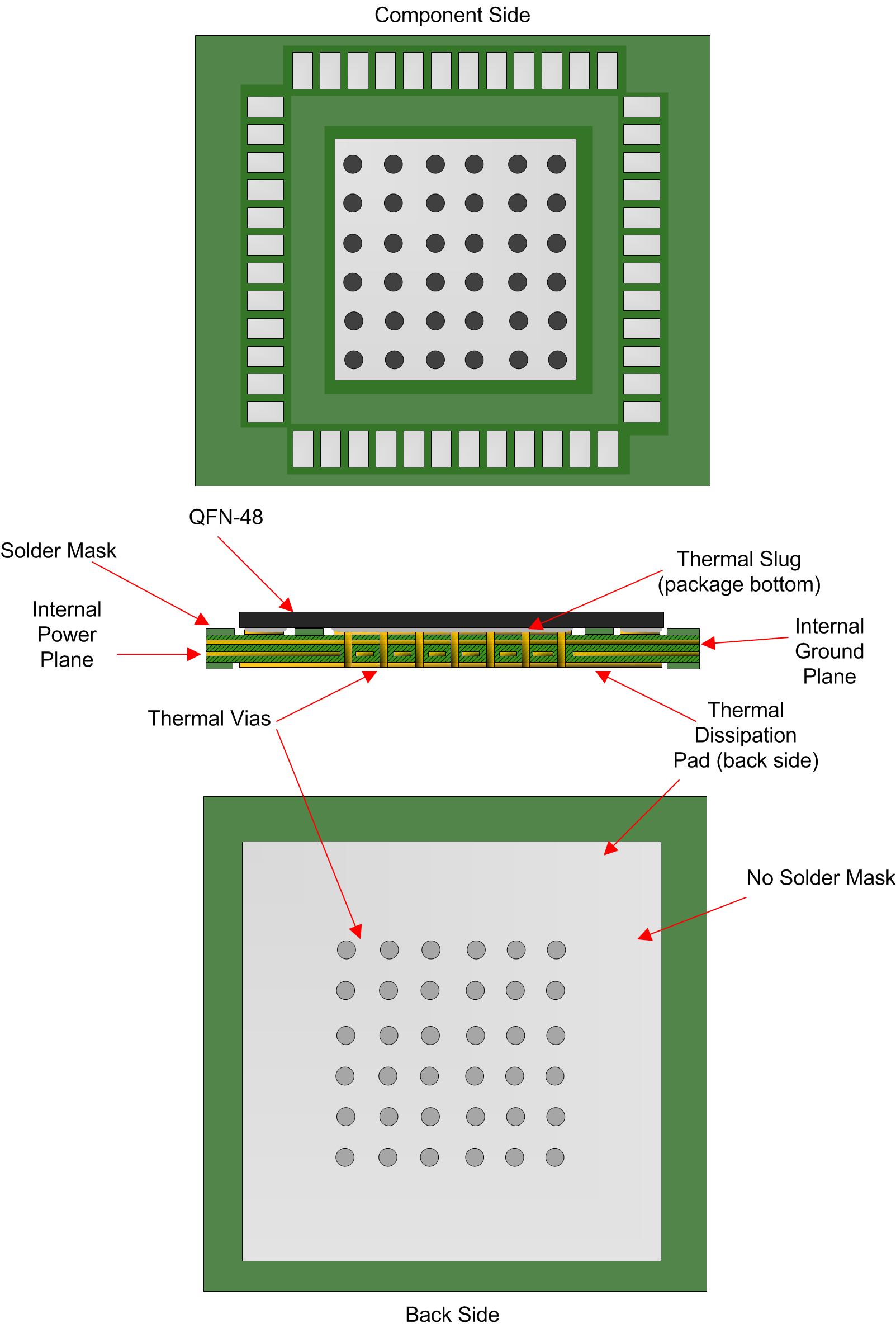
Layout Example
Figure 12-1
General PCB Ground Layout for Thermal Reliability (8+ Layers Recommended) - TBD
千亿体育app官网登录(中国)官方网站IOS/安卓通用版/手机APP
|
米乐app下载官网(中国)|ios|Android/通用版APP最新版
|
米乐|米乐·M6(中国大陆)官方网站
|
千亿体育登陆地址
|
华体会体育(中国)HTH·官方网站
|
千赢qy国际_全站最新版千赢qy国际V6.2.14安卓/IOS下载
|
18新利网v1.2.5|中国官方网站
|
bob电竞真人(中国官网)安卓/ios苹果/电脑版【1.97.95版下载】
|
千亿体育app官方下载(中国)官方网站IOS/安卓/手机APP下载安装
|