ZHCSFX5C December 2016 – December 2017 LMK60E0-156M , LMK60E0-212M , LMK60E2-100M , LMK60E2-125M , LMK60E2-156M , LMK60I2-100M , LMK60I2-322M
PRODUCTION DATA.
- 1 特性
- 2 应用
- 3 说明
- 4 修订历史记录
- 5 Pin Configuration and Functions
-
6 Specifications
- 6.1 Absolute Maximum Ratings
- 6.2 ESD Ratings
- 6.3 Recommended Operating Conditions
- 6.4 Thermal Information
- 6.5 Electrical Characteristics - Power Supply
- 6.6 LVPECL Output Characteristics
- 6.7 LVDS Output Characteristics
- 6.8 HCSL Output Characteristics
- 6.9 OE Input Characteristics
- 6.10 Frequency Tolerance Characteristics
- 6.11 Power-On/Reset Characteristics (VDD)
- 6.12 PSRR Characteristics
- 6.13 PLL Clock Output Jitter Characteristics
- 6.14 Additional Reliability and Qualification
- 7 Parameter Measurement Information
- 8 Power Supply Recommendations
- 9 Layout
- 10器件和文档支持
- 11机械、封装和可订购信息
7.1 Device Output Configurations
 Figure 1. LVPECL Output DC Configuration During Device Test
 Figure 2. LVDS Output DC Configuration During Device Test
 Figure 3. HCSL Output DC Configuration During Device Test (1)
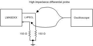
 Figure 4. LVPECL Output AC Configuration During Device Test
 Figure 5. LVDS Output AC Configuration During Device Test
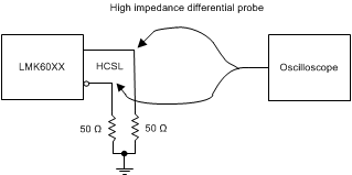
 Figure 6. HCSL Output AC Configuration During Device Test
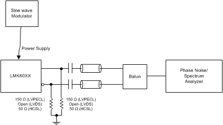
 Figure 7. PSRR Test Setup
 Figure 8. Differential Output Voltage and Rise/Fall Time
1. Also compatible with 85 Ω termination