ZHCSH74B december 2017 – august 2023 LMK61E07
PRODUCTION DATA
- 1
- 1 特性
- 2 应用
- 3 说明
- 4 Revision History
- 5 Pin Configuration and Functions
-
6 Specifications
- 6.1 Absolute Maximum Ratings
- 6.2 ESD Ratings
- 6.3 Recommended Operating Conditions
- 6.4 Thermal Information
- 6.5 Electrical Characteristics - Power Supply
- 6.6 LVPECL Output Characteristics
- 6.7 LVDS Output Characteristics
- 6.8 HCSL Output Characteristics
- 6.9 Frequency Tolerance Characteristics
- 6.10 Frequency Margining Characteristics
- 6.11 Power-On Reset Characteristics (VDD)
- 6.12 I2C-Compatible Interface Characteristics (SDA, SCL)
- 6.13 PSRR Characteristics
- 6.14 Other Characteristics
- 6.15 PLL Clock Output Jitter Characteristics
- 6.16 Typical 156.25-MHz Output Phase Noise Characteristics
- 6.17 Typical 161.1328125 MHz Output Phase Noise Characteristics
- 6.18 Additional Reliability and Qualification
- 6.19 Typical Characteristics
- 7 Parameter Measurement Information
-
8 Detailed Description
- 8.1 Overview
- 8.2 Functional Block Diagram
- 8.3
Feature Description
- 8.3.1 Device Block-Level Description
- 8.3.2 Device Configuration Control
- 8.3.3 Register File Reference Convention
- 8.3.4 Configuring the PLL
- 8.3.5 Integrated Oscillator
- 8.3.6 Reference Divider and Doubler
- 8.3.7 Phase Frequency Detector
- 8.3.8 Feedback Divider (N)
- 8.3.9 Fractional Engine
- 8.3.10 Charge Pump
- 8.3.11 Loop Filter
- 8.3.12 VCO Calibration
- 8.3.13 High-Speed Output Divider
- 8.3.14 High-Speed Clock Output
- 8.3.15 Device Status
- 8.4 Device Functional Modes
- 8.5 Programming
- 8.6
Register Maps
- 8.6.1
Register Descriptions
- 8.6.1.1 VNDRID_BY1 Register; R0
- 8.6.1.2 VNDRID_BY0 Register; R1
- 8.6.1.3 PRODID Register; R2
- 8.6.1.4 REVID Register; R3
- 8.6.1.5 TARGETADR Register; R8
- 8.6.1.6 EEREV Register; R9
- 8.6.1.7 DEV_CTL Register; R10
- 8.6.1.8 XO_CAPCTRL_BY1 Register; R16
- 8.6.1.9 XO_CAPCTRL_BY0 Register; R17
- 8.6.1.10 DIFFCTL Register; R21
- 8.6.1.11 OUTDIV_BY1 Register; R22
- 8.6.1.12 OUTDIV_BY0 Register; R23
- 8.6.1.13 RDIVCMOSCTL Register; R24
- 8.6.1.14 PLL_NDIV_BY1 Register; R25
- 8.6.1.15 PLL_NDIV_BY0 Register; R26
- 8.6.1.16 PLL_FRACNUM_BY2 Register; R27
- 8.6.1.17 PLL_FRACNUM_BY1 Register; R28
- 8.6.1.18 PLL_FRACNUM_BY0 Register; R29
- 8.6.1.19 PLL_FRACDEN_BY2 Register; R30
- 8.6.1.20 PLL_FRACDEN_BY1 Register; R31
- 8.6.1.21 PLL_FRACDEN_BY0 Register; R32
- 8.6.1.22 PLL_MASHCTRL Register; R33
- 8.6.1.23 PLL_CTRL0 Register; R34
- 8.6.1.24 PLL_CTRL1 Register; R35
- 8.6.1.25 PLL_LF_R2 Register; R36
- 8.6.1.26 PLL_LF_C1 Register; R37
- 8.6.1.27 PLL_LF_R3 Register; R38
- 8.6.1.28 PLL_LF_C3 Register; R39
- 8.6.1.29 PLL_CALCTRL Register; R42
- 8.6.1.30 NVMSCRC Register; R47
- 8.6.1.31 NVMCNT Register; R48
- 8.6.1.32 NVMCTL Register; R49
- 8.6.1.33 NVMLCRC Register; R50
- 8.6.1.34 MEMADR Register; R51
- 8.6.1.35 NVMDAT Register; R52
- 8.6.1.36 RAMDAT Register; R53
- 8.6.1.37 NVMUNLK Register; R56
- 8.6.1.38 INT_LIVE Register; R66
- 8.6.1.39 SWRST Register; R72
- 8.6.1
Register Descriptions
- 9 Application and Implementation
- 10Device and Documentation Support
- 11Mechanical, Packaging, and Orderable Information
8.4.1 Interface and Control
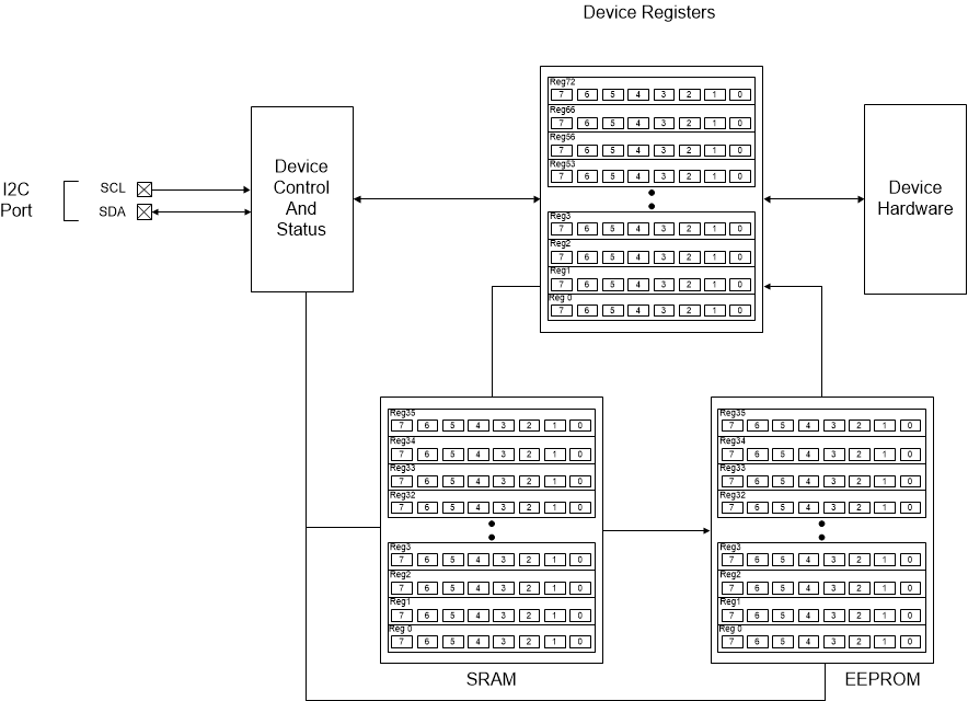
The host (DSP, Microcontroller, FPGA, and so forth) configures and monitors the LMK61E07 through the I2C port. The host reads and writes to a collection of control and status bits called the register map. The device blocks can be controlled and monitored through a specific grouping of bits located within the register file. The host controls and monitors certain device Wide critical parameters directly through register control and status bits. In the absence of the host, the LMK61E07 can be configured to operate from its on-chip EEPROM. The EEPROM array is automatically copied to the device registers upon power up. The user has the flexibility to rewrite the contents of EEPROM from the SRAM up to 100 times.
Within the device registers, there are certain bits that have read or write access. Other bits are read-only (an attempt to write to a read-only bit will not change the state of the bit). Certain device registers and bits are reserved meaning that they must not be changed from their default reset state. Figure 8-3 shows interface and control blocks within LMK61E07 and the arrows refer to read access from and write access to the different embedded memories (EEPROM, SRAM).
 Figure 8-3 LMK61E07 Interface and Control Block