ZHCSEB9A October 2015 – November 2015 LMK61PD0A2
PRODUCTION DATA.
- 1 特性
- 2 应用
- 3 说明
- 4 修订历史记录
- 5 Device Control
- 6 Pin Configuration and Functions
-
7 Specifications
- 7.1 Absolute Maximum Ratings
- 7.2 ESD Ratings
- 7.3 Recommended Operating Conditions
- 7.4 Thermal Information
- 7.5 Electrical Characteristics - Power Supply
- 7.6 LVPECL Output Characteristics
- 7.7 LVDS Output Characteristics
- 7.8 HCSL Output Characteristics
- 7.9 OE Input Characteristics
- 7.10 OS, FS[1:0] Input Characteristics
- 7.11 Frequency Tolerance Characteristics
- 7.12 Power-On/Reset Characteristics (VDD)
- 7.13 PSRR Characteristics
- 7.14 PLL Clock Output Jitter Characteristics
- 7.15 Additional Reliability and Qualification
- 7.16 Typical Performance Characteristics
- 8 Parameter Measurement Information
- 9 Detailed Description
- 10Application and Implementation
- 11Power Supply Recommendations
- 12Layout
- 13器件和文档支持
- 14机械、封装和可订购信息
9 Detailed Description
9.1 Overview
The LMK61PD0A2 is a pin selectable oscillator that generates commonly used reference clocks, greater than 100 MHz, with less than 200 fs, rms max random jitter.
9.2 Functional Block Diagram

NOTE
Control blocks are compatible with 1.8/2.5/3.3 V I/O voltage levels.
9.3 Feature Description
9.3.1 Device Block-Level Description
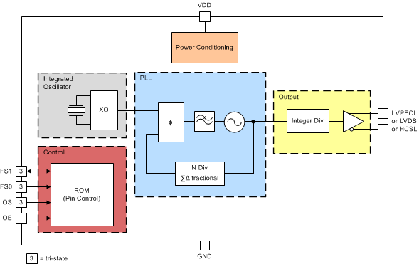
The LMK61PD0A2 comprises of an integrated oscillator that includes a 50 MHz crystal, a fractional PLL with integrated VCO. Completing the device is the combination of an integer output divider and a universal differential output buffer. The on-chip ROM contains seven pre-programmed output frequency plans that selects the appropriate settings for the integrated oscillator, PLL blocks and output divider. Table 1 lists the supported output frequency plans that can be selected by pin-strapping FS[1:0] as required. Table 2 lists the supported output types that can be selected by pin-strapping OS and OE as required. The device is powered by on-chip low dropout (LDO) linear voltage regulators and the regulated supply network is partitioned such that the sensitive analog supplies are running from separate LDOs than the digital supplies which use their own LDO. The LDOs provide isolation from any noise in the external power supply rail with a PSRR of better than -70 dBc at 50 kHz to 1 MHz ripple frequencies at 3.3 V device supply.
9.3.2 Device Configuration Control
The LMK61PD0A2 selects an output frequency plan and output type using control pins FS[1:0].