ZHCSEB9A October 2015 – November 2015 LMK61PD0A2
PRODUCTION DATA.
- 1 特性
- 2 应用
- 3 说明
- 4 修订历史记录
- 5 Device Control
- 6 Pin Configuration and Functions
-
7 Specifications
- 7.1 Absolute Maximum Ratings
- 7.2 ESD Ratings
- 7.3 Recommended Operating Conditions
- 7.4 Thermal Information
- 7.5 Electrical Characteristics - Power Supply
- 7.6 LVPECL Output Characteristics
- 7.7 LVDS Output Characteristics
- 7.8 HCSL Output Characteristics
- 7.9 OE Input Characteristics
- 7.10 OS, FS[1:0] Input Characteristics
- 7.11 Frequency Tolerance Characteristics
- 7.12 Power-On/Reset Characteristics (VDD)
- 7.13 PSRR Characteristics
- 7.14 PLL Clock Output Jitter Characteristics
- 7.15 Additional Reliability and Qualification
- 7.16 Typical Performance Characteristics
- 8 Parameter Measurement Information
- 9 Detailed Description
- 10Application and Implementation
- 11Power Supply Recommendations
- 12Layout
- 13器件和文档支持
- 14机械、封装和可订购信息
12 Layout
12.1 Layout Guidelines
The following sections provides recommendations for board layout, solder reflow profile and power supply bypassing when using LMK61PD0A2 to ensure good thermal / electrical performance and overall signal integrity of entire system.
12.1.1 Ensuring Thermal Reliability
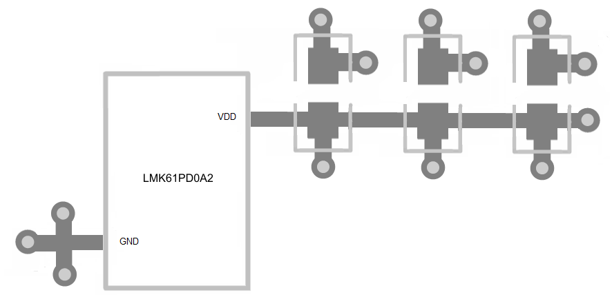
The LMK61PD0A2 is a high performance device. Therefore careful attention must be paid to device configuration and printed circuit board (PCB) layout with respect to power consumption. The ground pin needs to be connected to the ground plane of the PCB through three vias or more, as shown in Figure 16, to maximize thermal dissipation out of the package.
Equation 1 describes the relationship between the PCB temperature around the LMK61PD0A2 and its junction temperature.
where
- TB: PCB temperature around the LMK61PD0A2
- TJ: Junction temperature of LMK61PD0A2
- ΨJB: Junction-to-board thermal resistance parameter of LMK61PD0A2 (36.7°C/W without airflow)
- P: On-chip power dissipation of LMK61PD0A2
In order to ensure that the maximum junction temperature of LMK61PD0A2 is below 125°C, it can be calculated that the maximum PCB temperature without airflow should be at 100°C or below when the device is optimized for best performance resulting in maximum on-chip power dissipation of 0.68 W.
12.1.2 Best Practices for Signal Integrity
For best electrical performance and signal integrity of entire system with LMK61PD0A2, it is recommended to route vias into decoupling capacitors and then into the LMK61PD0A2. It is also recommended to increase the via count and width of the traces wherever possible. These steps ensure lowest impedance and shortest path for high frequency current flow. Figure 16 shows the layout recommendation for LMK61PD0A2.
 Figure 16. LMK61PD0A2 Layout Recommendation for Power Supply and Ground
12.1.3 Recommended Solder Reflow Profile
It is recommended to follow the solder paste supplier's recommendations to optimize flux activity and to achieve proper melting temperatures of the alloy within the guidelines of J-STD-20. It is preferrable for the LMK61PD0A2 to be processed with the lowest peak temperature possible while also remaining below the components peak temperature rating as listed on the MSL label. The exact temperature profile would depend on several factors including maximum peak temperature for the component as rated on the MSL label, Board thickness, PCB material type, PCB geometries, component locations, sizes, densities within PCB, as well solder manufactures recommended profile, and capability of the reflow equipment to as confirmed by the SMT assembly operation.