SNVSAL6A July 2016 – February 2017 LMP8480-Q1 , LMP8481-Q1
PRODUCTION DATA.
- 1 Features
- 2 Applications
- 3 Description
- 4 Revision History
- 5 Device Comparison Table
- 6 Pin Configuration and Functions
- 7 Specifications
-
8 Detailed Description
- 8.1 Overview
- 8.2 Functional Block Diagrams
- 8.3
Feature Description
- 8.3.1 Basic Connections
- 8.3.2 Selection of the Sense Resistor
- 8.3.3 Using PCB Traces as Sense Resistors
- 8.3.4 VREFA and VREFB Pins (LMP8481-Q1 Only)
- 8.3.5 Reference Input Voltage Limits (LMP8481-Q1 Only)
- 8.3.6 Low-Side Current Sensing
- 8.3.7 Input Series Resistance
- 8.3.8 Minimum Output Voltage
- 8.3.9 Swinging Output Below Ground
- 8.3.10 Maximum Output Voltage
- 8.4 Device Functional Modes
- 9 Application and Implementation
- 10Power Supply Recommendations
- 11Layout
- 12Device and Documentation Support
- 13Mechanical, Packaging, and Orderable Information
6 Pin Configuration and Functions
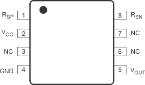
DGK Package, LMP8480-Q1
8-Pin VSSOP
Top View

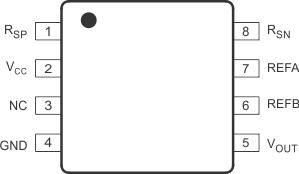
DGK Package, LMP8481-Q1
8-Pin VSSOP
Top View

Pin Functions
| PIN | I/O | DESCRIPTION | ||
|---|---|---|---|---|
| NAME | NO. | |||
| LMP8480-Q1 | LMP8481-Q1 | |||
| GND | 4 | 4 | P | Ground |
| NC | 3, 6, 7 | 3 | — | No connection, not internally connected |
| REFA | — | 7 | I | Reference voltage A input |
| REFB | — | 6 | I | Reference voltage B input |
| RSN | 8 | 8 | I | Negative current-sense input |
| RSP | 1 | 1 | I | Positive current-sense input |
| VCC | 2 | 2 | P | Positive supply voltage |
| VOUT | 5 | 5 | O | Output |