ZHCSFO1H September 2008 – April 2016 LMP8601 , LMP8601-Q1 , LMP8602 , LMP8602-Q1 , LMP8603 , LMP8603-Q1
PRODUCTION DATA.
- 1 特性
- 2 应用
- 3 说明
- 4 修订历史记录
- 5 Pin Configuration and Functions
- 6 Specifications
- 7 Detailed Description
- 8 Application and Implementation
- 9 Power Supply Recommendations
- 10Layout
- 11器件和文档支持
- 12机械、封装和可订购信息
8 Application and Implementation
NOTE
Information in the following applications sections is not part of the TI component specification, and TI does not warrant its accuracy or completeness. TI’s customers are responsible for determining suitability of components for their purposes. Customers should validate and test their design implementation to confirm system functionality.
8.1 Application Information
8.1.1 Specifying Performance
To specify the high performance of the LMP860x and LMP860x-Q1, all minimum and maximum values shown in the parameter tables of this data sheet are 100% tested, and all over temperature limits are also 100% tested over temperature.
8.2 Typical Applications
8.2.1 High-Side, Current-Sensing Application
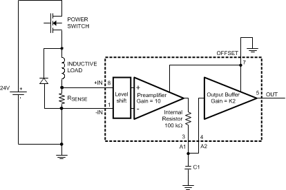
Figure 60 illustrates the application of the LMP860x and LMP860x-Q1 in a high-side sensing application. This application is similar to the low-side sensing discussed below, except in this application the common-mode voltage on the shunt drops below ground when the driver is switched off. Because the common-mode voltage range of the LMP860x and LMP860x-Q1 extends below the negative rail, the LMP860x and LMP860x-Q1 are also very well suited for this application.
8.2.1.1 Design Requirements
Using the circuit in Figure 60, the requirement is to measure coil current up to 10 A and drive the ADC input to a maximum of 3.3 V. The OFFSET pin is grounded, so zero current will result in a zero volt output.
8.2.1.2 Detailed Design Procedure
First, the value of RSENSE must be determined. RSENSE can be found by dividing the maximum desired output swing by the gain to determine the maximum input voltage. In this example, the LMP8601 is used, with a gain of 20 V/V, as shown in Equation 33:

Knowing 165 mV must be generated, the ideal value of the sense resistor can be determined through simple ohms law:

The ideal sense resistor value is 16.5 mΩ. The closest standard value is 15 mΩ, but this value may cause the output to slightly overrange at 10 V. It is recommended to reduce the expected maximum output by a few percent to allow for overloads and component tolerances. The next most popular values would be 10 mΩ, 15 mΩ, and 20 mΩ. 10 mΩ allows for a maximum output of 2 V at 10 A, but may be too low and not use the full output range. 20 mΩ provides more sensitivity, but limits the maximum current to 8.25 A. 15 mΩ is a good compromise at 11 A maximum, and allows for some component tolerance variation.
If a suitable sense resistor value is not available, it is possible to adjust the gain as detailed in the Gain Adjustment section.
The sense resistor does dissipates power, so the maximum wattage rating and appropriate power deratings must be observed. In the example above, the sense resistor dissipates 0.165 V × 10 A = 1.65 W, so a sense resistor of at least twice the maximum expected power should be used (greater than 4 W).
8.2.1.3 Application Curve
Below is the expected output value using a 15-mΩ sense resistor.
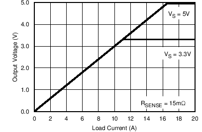 Figure 61. Expected Output Voltage vs Load Current Using 15-mΩ Sense Resistor
8.2.2 Low-Side, Current-Sensing Application
Figure 62 illustrates a low-side, current-sensing application with a low-side driver. The power transistor is pulse width modulated to control the average current flowing through the inductive load which is connected to a relatively high battery voltage. The current through the load is measured across a shunt resistor RSENSE in series with the load. When the power transistor is on, current flows from the battery through the inductive load, the shunt resistor and the power transistor to ground. In this case, the common-mode voltage on the shunt is close to ground. When the power transistor is off, current flows through the inductive load, through the shunt resistor and through the freewheeling diode. In this case the common-mode voltage on the shunt is at least one diode voltage drop above the battery voltage. Therefore, in this application the common-mode voltage on the shunt is varying between a large positive voltage and a relatively low voltage. Because the large common-mode voltage range of the LMP860x and LMP860x-Q1 and because of the high ac common-mode rejection ratio, the LMP860x and LMP860x-Q1 are very well suited for this application.
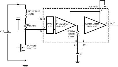
For this application, the following example can be used for the calculation of the sense voltage (VSENSE):
When using a sense resistor, RSENSE, of 0.01 Ω and a current, ILOAD, of 1 A, the sense voltage at the input pins of the LMP860x and LMP860x-Q1 is:
With the gain of 20 for the LMP8601, the result is an output of 0.2 V. Or in other words, VOUT = 0.2 V/A. The result is the same for the LMP8601-Q1.
For the LMP8602 and LMP8602-Q1 with a gain of 50, the output is 0.5 V/A.
For the LMP8603 and LMP8603-Q1 with a gain of 100, the output is 1 V/A.
8.2.3 Battery Current Monitor Application
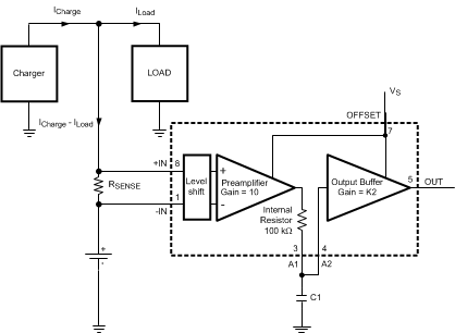
This application example shows how the LMP860x and LMP860x-Q1 can be used to monitor the current flowing in and out of a battery pack. The fact that the LMP860x and LMP860x-Q1 can measure small voltages at a high offset voltage outside the parts own supply range makes this part a very good choice for such applications. If the load current of the battery is higher then the charging current, the output voltage of the LMP860x and LMP860x-Q1 will be above the half offset voltage for a net current flowing out of the battery. When the charging current is higher then the load current the output will be below this half offset voltage.
8.2.4 Advanced Battery Charger Application
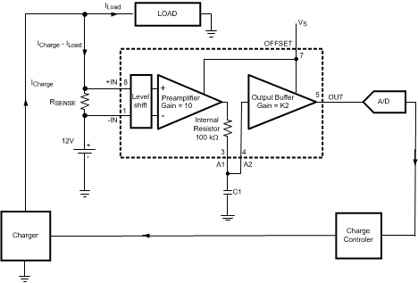
Figure 63 can be used to realize an advanced battery charger that has the capability to monitor the exact net current that flows in and out the battery as show in Figure 64. The output signal of the LMP860x and LMP860x-Q1 is digitized with the ADC and used as an input for the charge controller. The Charge controller can be used to regulate the charger circuit to deliver exactly the current that is required by the load, avoiding overcharging a fully loaded battery.
8.2.5 Current Loop Receiver Application
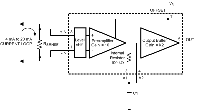
Many industrial applications use 4-mA to 20-mA transmitters to send an analog value of a sensor to a central control room. The LMP860x and LMP860x-Q1 can be used as a current loop receiver as shown in Figure 65.
