ZHCSQG1H November   2009  – May 2022 LMP8645 , LMP8645HV

PRODUCTION DATA  

  1. 特性
  2. 应用
  3. 说明
  4. Revision History
  5. Pin Configuration and Functions
  6. Specifications
    1. 6.1 Absolute Maximum Ratings
    2. 6.2 ESD Ratings
    3. 6.3 Recommended Operating Conditions
    4. 6.4 Thermal Information
    5. 6.5 2.7-V Electrical Characteristics
    6. 6.6 5-V Electrical Characteristics
    7. 6.7 12-V Electrical Characteristics
    8. 6.8 Typical Characteristics
  7. Detailed Description
    1. 7.1 Overview
      1. 7.1.1 Theory of Operation
    2. 7.2 Functional Block Diagram
    3. 7.3 Feature Description
      1. 7.3.1 Driving ADC
      2. 7.3.2 Applying Input Voltage With No Supply Voltage
    4. 7.4 Device Functional Modes
      1. 7.4.1 Selection of the Gain Resistor
      2. 7.4.2 Gain Range Limitations
        1. 7.4.2.1 Range 1: VCM is –2 V to 1.8 V
        2. 7.4.2.2 Range 2: VCM is 1.8 V to VS
        3. 7.4.2.3 Range 3: VCM is greater than VS
      3. 7.4.3 Selection of Sense Resistor
        1. 7.4.3.1 Resistor Power Rating and Thermal Issues
        2. 7.4.3.2 Using PCB Trace as a Sense Resistor
      4. 7.4.4 Sense Line Inputs
        1. 7.4.4.1 Effects of Series Resistance on Sense Lines
  8. Application and Implementation
    1. 8.1 Application Information
    2. 8.2 Typical Applications
      1. 8.2.1 Typical Current Monitor Application
        1. 8.2.1.1 Design Requirements
        2. 8.2.1.2 Detailed Design Procedure
        3. 8.2.1.3 Application Curves
      2. 8.2.2 High Brightness LED Driver
  9. Power Supply Recommendations
  10. 10Layout
    1. 10.1 Layout Guidelines
    2. 10.2 Layout Example
  11. 11Device and Documentation Support
    1. 11.1 Device Support
      1. 11.1.1 Development Support
    2. 11.2 Documentation Support
      1. 11.2.1 Related Documentation
    3. 11.3 接收文档更新通知
    4. 11.4 支持资源
    5. 11.5 Trademarks
    6. 11.6 Electrostatic Discharge Caution
    7. 11.7 术语表
  12. 12Mechanical, Packaging, and Orderable Information

封装选项

机械数据 (封装 | 引脚)
散热焊盘机械数据 (封装 | 引脚)
订购信息

Theory of Operation

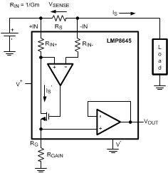
GUID-C5EAB2E3-BD7E-482E-A444-B0E0B4D80483-low.gifFigure 7-1 Current Monitor Example Circuit

As seen in Figure 7-1, the current flowing through the shunt resistor ( RS) develops a voltage drop equal to VSENSE across RS. The resulting voltage at the –IN pin will now be less than +IN pin proportional to the VSENSE voltage.

The sense amplifier senses this indifference and increases the gate drive to the MOSFET to increase IS′ current flowing through the RIN+ string until the amplifer inputs are equal. In this way, the voltage drop across RIN+ now matches the votlage drop across VSENSE.

The RIN resistors are trimmed to a nominal value of 5 kΩ each. The current IS′ flows through RIN+ , the MOSFET, and RGAIN to ground. The IS′ current generates the voltage VG across RGAIN. The gain is created bythe ratio of RGAIN and RIN.

A current proportional to IS is generated according to the following relation:

Equation 1. IS′ = VSENSE / RIN = RS × IS / RIN

where

  • RIN = 1 / Gm

This current flows entirely in the external gain resistor developing a voltage drop equal to:

Equation 2. VG = IS′ × RGAIN = (VSENSE / RIN) × RGAIN = ( (RS × IS) / RIN ) × RGAIN

This voltage is buffered and presented at the output with a very low output impedance allowing a very easy interface to other devices (ADC, μC…).

Equation 3. VOUT = (RS × IS) × G

where

  • G = RGAIN / RIN