ZHCSQG1H November 2009 – May 2022 LMP8645 , LMP8645HV
PRODUCTION DATA
- 1 特性
- 2 应用
- 3 说明
- 4 Revision History
- 5 Pin Configuration and Functions
- 6 Specifications
- 7 Detailed Description
- 8 Application and Implementation
- 9 Power Supply Recommendations
- 10Layout
- 11Device and Documentation Support
- 12Mechanical, Packaging, and Orderable Information
7.4.3 Selection of Sense Resistor
The accuracy of the current measurement highly depends on the value of the shunt resistor RS. Its value depends on the application and it is a compromise between small-signal accuracy and maximum permissible voltage (and power) loss in the sense resistor. High values of RS provide better accuracy at lower currents by minimizing the effects of amplifier offset. Low values of RS minimize voltage and power loss in the supply section, but at the expense of low current accuracy. For most applications, best performance is obtained with an RS value that provides a full-scale shunt voltage range of 100 mV to 200 mV.
In applications where a small current is sensed, a larger value of RS is selected to minimize the error in the proportional output voltage. Higher resistor value improves the signal-to-noise ratio (SNR) at the input of the current sense amplifier and hence gives a more accurate output.
Similarly when high current is sensed, the power losses in RS can be significant so a smaller value of RS is desired. In this condition it is also required to take in account also the power rating of RS resistor. The low input offset and customizable gain of the LMP8645 allows the use of small sense resistors to reduce power dissipation still providing a good input dynamic range. The input dynamic range is the ratio between the maximum signal that can be measured and the minimum signal that can be detected, where usually the input offset and amplifier noise are the principal limiting factors.
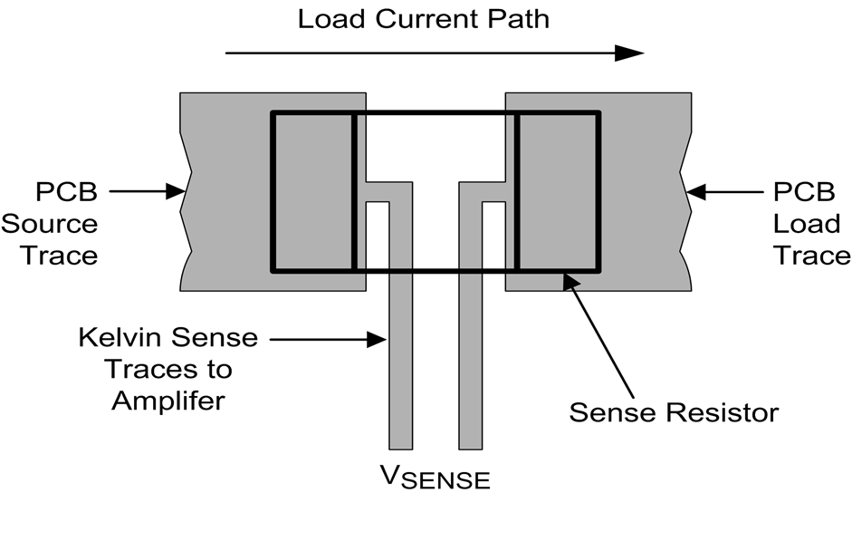
 Figure 7-6 Example of a Kelvin (4-Wire) Connection to a Two-Terminal Resistor
The amplifier inputs should be directly connected to the sense resistor pads using Kelvin or 4-wire connection techniques. The paths of the input traces should be identical, including connectors and vias, so that these errors will be equal and cancel.