ZHCSDM7B February   2012  – December 2014 LMP8646

PRODUCTION DATA.  

  1. 特性
  2. 应用
  3. 说明
  4. 修订历史记录
  5. Pin Configuration and Functions
  6. Specifications
    1. 6.1 Absolute Maximum Ratings
    2. 6.2 ESD Ratings
    3. 6.3 Recommended Operating Conditions
    4. 6.4 Thermal Information
    5. 6.5 Electrical Characteristics: 2.7 V
    6. 6.6 Electrical Characteristics: 5 V
    7. 6.7 Electrical Characteristics: 12 V
    8. 6.8 Typical Characteristics
  7. Detailed Description
    1. 7.1 Overview
    2. 7.2 Functional Block Diagram
    3. 7.3 Feature Description
      1. 7.3.1 Theory of Operation
        1. 7.3.1.1 Maximum Output Voltage, VOUT_MAX
          1. 7.3.1.1.1 Case 1: −2 V < VCM < 1.8 V, and VS > 2.7 V
          2. 7.3.1.1.2 Case 2: 1.8 V < VCM < VS, and VS > 3.3 V
          3. 7.3.1.1.3 Case 3: VCM > VS, and VS > 2.7 V
    4. 7.4 Device Functional Modes
      1. 7.4.1 Output Accuracy
      2. 7.4.2 Selection of the Sense Resistor, RSENSE
        1. 7.4.2.1 RSENSE Consideration for System Error
  8. Application and Implementation
    1. 8.1 Application Information
    2. 8.2 Typical Applications
      1. 8.2.1 Application #1: Current Limiter With a Capacitive Load
        1. 8.2.1.1 Design Requirements
        2. 8.2.1.2 Detailed Design Procedure
        3. 8.2.1.3 Application Curve
      2. 8.2.2 Application #2: Current Limiter With a Resistive Load
        1. 8.2.2.1 Design Requirements
        2. 8.2.2.2 Detailed Design Procedure
        3. 8.2.2.3 Application Curve
      3. 8.2.3 Application #3: Current Limiter With a Low-Dropout Regulator and Resistive Load
        1. 8.2.3.1 Design Requirements
        2. 8.2.3.2 Detailed Design Procedure
        3. 8.2.3.3 Application Curve
  9. Power Supply Recommendations
  10. 10Layout
    1. 10.1 Layout Guidelines
    2. 10.2 Layout Example
  11. 11器件和文档支持
    1. 11.1 商标
    2. 11.2 静电放电警告
    3. 11.3 Glossary
  12. 12机械、封装和可订购信息

封装选项

机械数据 (封装 | 引脚)
散热焊盘机械数据 (封装 | 引脚)
订购信息

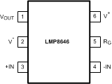
5 Pin Configuration and Functions

DDC Package
6-Pin SOT
Top View
LMP8646 30123502.gif

Pin Functions

PIN DESCRIPTION
NAME NO.
VOUT 1 Single-Ended Output Voltage
V- 2 Negative Supply Voltage. This pin should be connected to ground.
+IN 3 Positive Input
-IN 4 Negative Input
RG 5 External Gain Resistor. An external capacitance (CG) may be added in parallel with RG to limit the bandwidth.
V+ 6 Positive Supply Voltage