ZHCS587H July 2011 – January 2016 LMP90077 , LMP90078 , LMP90079 , LMP90080
PRODUCTION DATA.
- 1 特性
- 2 应用
- 3 说明
- 4 修订历史记录
- 5 说明 (续)
- 6 Device Comparison Table
- 7 Pin Configuration and Functions
-
8 Specifications
- 8.1 Absolute Maximum Ratings
- 8.2 ESD Ratings
- 8.3 Recommended Operating Conditions
- 8.4 Thermal Information
- 8.5 Electrical Characteristics
- 8.6 Timing Requirements
- 8.7 Timing Requirements - CSB Timing
- 8.8 Timing Requirements - SCLK and SDI Timing
- 8.9 Timing Requirements - SDO Timing With DOD1
- 8.10 Timing Requirements - SDO Timing with DOD2
- 8.11 Timing Requirements - SDO and DRDYB Timing
- 8.12 Typical Characteristics
-
9 Detailed Description
- 9.1 Overview
- 9.2 Functional Block Diagram
- 9.3
Feature Description
- 9.3.1 Calibration
- 9.3.2 True Continuous Background Calibration
- 9.3.3 Continuous Background Sensor Diagnostics
- 9.3.4 Flexible Input MUX Channels
- 9.3.5 Programmable Gain Amplifiers (FGA & PGA)
- 9.3.6 Excitation Current Sources (IB1 & IB2) - LMP90080/LMP90078
- 9.3.7 Signal Path
- 9.4 Device Functional Modes
- 9.5
Programming
- 9.5.1 Serial Digital Interface
- 9.5.2 RESET and RESTART
- 9.5.3 Register Read/Write Examples
- 9.5.4 Streaming Examples
- 9.6 Register Maps
- 10Application and Implementation
- 11Power Supply Recommendations
- 12Layout
- 13器件和文档支持
- 14机械、封装和可订购信息
9 Detailed Description
9.1 Overview
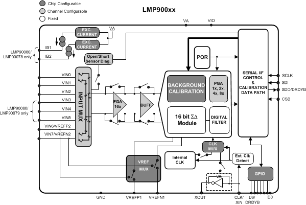
Throughout this datasheet, the LMP90080/LMP90079/LMP90078/LMP90077 will be referred to as the LMP900xx.
The LMP900xx is a low-power 16-Bit ΣΔ ADC with 4 fully differential/7 single-ended analog channels for the LMP90080/LMP90079 and 2 full differential/4 single-ended for the LMP90078/LMP90077. Its serial data output is two’s complement format. The output data rate (ODR) ranges from 1.6775 SPS to 214.65 SPS.
The serial communication for LMP900xx is SPI, a synchronous serial interface that operates using 4 pins: chip select bar (CSB), serial clock (SCLK), serial data in (SDI), and serial data out / data ready bar (SDO/DRDYB).
True continuous built-in offset and gain background calibration is also available to improve measurement accuracy. Unlike other ADCs, the LMP900xx’s background calibration can run without heavily impacting the input signal. This unique technique allows for positive as well as negative gain calibration and is available at all gain settings.
The registers can be found in the Register Maps section, and a detailed description of the LMP900xx are provided in the following sections.
9.2 Functional Block Diagram
9.3 Feature Description
9.3.1 Calibration
As seen in Figure 39, there are two types of calibration: background calibration and system calibration. These calibrations are further described in the next sections.
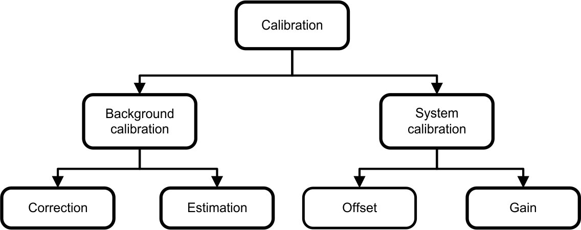 Figure 39. Types of Calibration
9.3.1.1 Background Calibration
Background calibration is the process of continuously determining and applying the offset and gain calibration coefficients to the output codes to minimize the LMP900xx’s offset and gain errors. Background calibration is a feature built into the LMP900xx and is automatically done by the hardware without interrupting the input signal.
Four differential channels, CH0-CH3, each with its own gain and ODRs, can be calibrated to improve the accuracy.
9.3.1.1.1 Types of Background Calibration:
Figure 39 also shows that there are two types of background calibration:
-
Type 1: Correction the process of continuously determining and applying the offset and gain calibration coefficients to the output codes to minimize the LMP900xx’s offset and gain errors.
This method keeps track of changes in the LMP900xx's gain and offset errors due to changes in the operating condition such as voltage, temperature, or time.
-
Type 2: Estimation the process of determining and continuously applying the last known offset and gain calibration coefficients to the output codes to minimize the LMP900xx’s offset and gain errors.
The last known offset or gain calibration coefficients can come from two sources. The first source is the default coefficient which is pre-determined and burnt in the device’s non-volatile memory. The second source is from a previous calibration run of Type 1: Correction.
The benefits of using Type 2 calibration is a higher throughput, lower power consumption, and slightly better noise. The exact savings would depend on the number of channels being scanned, and the ODR and gain of each channel.
9.3.1.1.2 Using Background Calibration:
There are four modes of background calibration, which can be programmed using the BGCALCN bits. They are as follows:
- BgcalMode0: Background Calibration OFF
- BgcalMode1: Offset Correction / Gain Estimation
- BgcalMode2: Offset Correction / Gain Correction. Follow Figure 40 to set other appropriate registers when using this mode.
- BgcalMode3: Offset Estimation / Gain Estimation
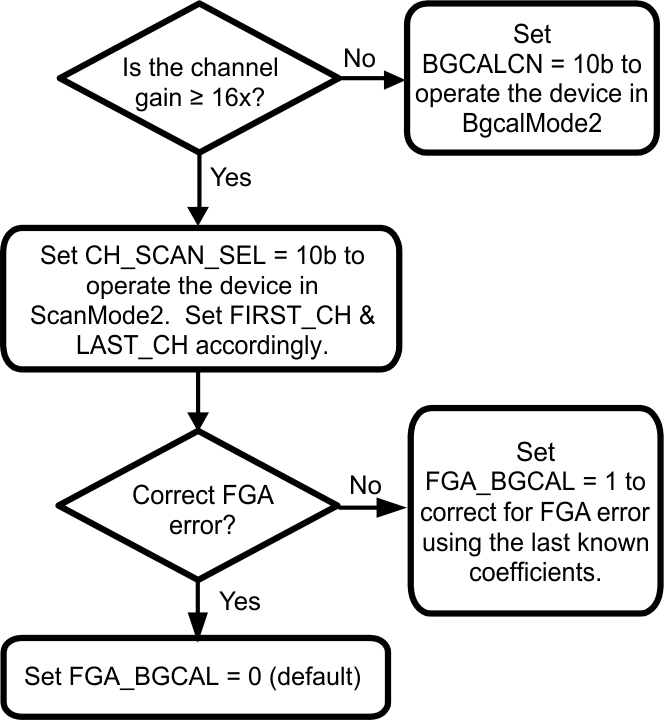 Figure 40. BgcalMode2 Register Settings
If operating in BgcalMode2, four channels (with the same ODR) are being converted, and FGA_BGCAL = 0 (default), then the ODR is reduced by:
- 0.19% of 1.6775 SPS
- 0.39% of 3.355 SPS
- 0.78% of 6.71 SPS
- 1.54% of 13.42 SPS
- 3.03% of 26.83125 SPS
- 5.88% of 53.6625 SPS
- 11.11% of 107.325 SPS
- 20% of 214.65 SPS
9.3.1.2 System Calibration
The LMP900xx provides some unique features to support easy system offset and system gain calibrations.
The System Calibration Offset Registers (CHx_SCAL_OFFSET) hold the System Calibration Offset Coefficients in 16-bit, two's complement binary format. The System Calibration Gain Registers (CHx_SCAL_GAIN) hold the System Calibration Gain Coefficient in 16-bit, 1.15, unsigned, fixed-point binary format. For each channel, the System Calibration Offset coefficient is subtracted from the conversion result prior to the division by the System Calibration Gain coefficient.
A data-flow diagram of these coefficients can be seen in Figure 41.
 Figure 41. System Calibration Data-Flow Diagram
There are four distinct sets of System Calibration Offset and System Calibration Gain Registers for use with CH0-CH3. CH4-CH6 reuse the registers of CH0-CH2, respectively.
The LMP900xx provides two system calibration modes that automatically fill the Offset and Gain coefficients for each channel. These modes are the System Calibration Offset Coefficient Determination mode and the System Calibration Gain Coefficient Determination mode. The System Calibration Offset Coefficient Determination mode must be entered prior to the System Calibration Gain Coefficient Determination mode, for each channel.
The system zero-scale condition is a system input condition (sensor loading) for which zero (0x0000) system-calibrated output code is desired. It may not, however, cause a zero input voltage at the input of the ADC.
The system reference-scale condition is usually the system full-scale condition in which the system's input (or sensor's loading) would be full-scale and the desired system-calibrated output code would be 0x8000 (unsigned 16-bit binary). However, system full-scale condition need not cause full-scale input voltage at the input of the ADC.
The system reference-scale condition is not restricted to just the system full-scale condition. In fact, it can be any arbitrary fraction of full-scale (up to 1.25 times) and the desired system-calibrated output code can be any appropriate value (up to 0xA000). The CHx_SCAL_GAIN register must be written with the desired system-calibrated output code (default:0x8000) before entering the System Calibration Gain Coefficient Determination mode. This helps in in-place system calibration.
9.3.1.2.1 System Calibration Offset Coefficient Determination Mode
Below are the detailed procedures for using the System Calibration Offset Coefficient Determination and System Calibration Gain Coefficient Determination modes.
- Apply system zero-scale condition to the channel (CH0/CH1/CH2/CH3).
- Enter the System Calibration Offset Coefficient Determination mode by programming 0x1 in the SCALCN register.
- LMP900xx starts a fresh conversion at the selected output data rate for the selected channel. At the end of the conversion, the CHx_SCAL_OFFSET register is filled-in with the System Calibration Offset coefficient.
- The System Calibration Offset Coefficient Determination mode is automatically exited.
- The computed calibration coefficient is accurate only to the effective resolution of the device and will probably contain some noise. The noise factor can be minimized by computing over many times, averaging (externally) and putting the resultant value back into the register. Alternatively, select the output data rate to be 26.83 SPS or 1.67 SPS.
9.3.1.2.2 System Calibration Gain Coefficient Determination Mode
- Repeat the System Calibration Offset Coefficient Determination to calibrate the System offset for the channel.
- Apply the system reference-scale condition to the channel CH0/CH1/CH2/CH3.
- In the CHx_SCAL_GAIN register, program the expected (desired) system-calibrated output code for this condition in 16-bit unsigned format.
- Enter the System Calibration Gain Coefficient Determination mode by programming 0x3 in the SCALCN register.
- LMP900xx starts a fresh conversion at the selected output data rate for the channel. At the end of the conversion, the CHx_SCAL_GAIN is filled-in (or overwritten) with the System Calibration Gain coefficient.
- The System Calibration Gain Coefficient Determination mode is automatically exited.
- The computed calibration coefficient is accurate only to the effective resolution of the device and will probably contain some noise. The noise factor can be minimized by computing over many times, averaging (externally) and putting the resultant value back into the register. Alternatively, select the output data rate to be 26.83 SPS or 1.67 SPS.
9.3.1.2.3 Post-Calibration Scaling
LMP900xx allows scaling (multiplication and shifting) for the System Calibrated result. This eases downstream processing, if any. Multiplication is done using the System Calibration Scaling Coefficient in the CHx_SCAL_SCALING register and shifting is done using the System Calibration Bits Selector in the CHx_SCAL_BITS_SELECTOR register.
The System Calibration Bits Selector value should ideally be the logarithm (to the base 2) of the System Calibration Scaling Coefficient value.
There are four distinct sets of System Calibration Scaling and System Calibration Bits Selector Registers for use with CH0-CH3. CH4-CH6 reuse the registers of CH0-CH2, respectively.
A data-flow diagram of these coefficients can be seen in Figure 42.
 Figure 42. Post-Calibration Scaling Data-Flow Diagram
9.3.2 True Continuous Background Calibration
The LMP90080/LMP90079/LMP90078/LMP90077 feature a 16-bit ΣΔ core with continuous background calibration to compensate for gain and offset errors in the ADC, virtually eliminating any drift with time and temperature. The calibration is performed in the background without user or ADC input interruption, making it unique in the industry and eliminating down time associated with field calibration required with other solutions. Having this continuous calibration improves performance over the entire life span of the end product.
9.3.3 Continuous Background Sensor Diagnostics
Sensor diagnostics are also performed in the background, without interfering with signal path performance, allowing the detection of sensor shorts, opens, and out-of-range signals, which vastly improves system reliability. In addition, the fully flexible input multiplexer described below allows any input pin to be connected to any ADC input channel providing additional sensor path diagnostic capability.
9.3.4 Flexible Input MUX Channels
The flexible input MUX allows interfacing to a wide range of sensors such as thermocouples, RTDs, thermistors, and bridge sensors. The LMP90080/LMP90079’s multiplexer supports 4 differential channels while the LMP90078/LMP90077 supports 2. Each effective input voltage that is digitized is VIN = VINX – VINY, where x and y are any input. In addition, the input multiplexer of the LMP90080/LMP90079 also supports 7 single-ended channels (LMP90078/LMP90077 supports 4), where the common ground is any one of the inputs.
9.3.5 Programmable Gain Amplifiers (FGA & PGA)
The LMP90080/LMP90079/LMP90078/LMP90077 contain an internal 16x fixed gain amplifier (FGA) and a 1x, 2x, 4x, or 8x programmable gain amplifier (PGA). This allows accurate gain settings of 1x, 2x, 4x, 8x, 16x, 32x, 64x, or 128x through configuration of internal registers. Having an internal amplifier eliminates the need for external amplifiers that are costly, space consuming, and difficult to calibrate.
9.3.6 Excitation Current Sources (IB1 & IB2) - LMP90080/LMP90078
Two matched internal excitation currents, IB1 and IB2, can be used for sourcing currents to a variety of sensors. The current range is from 100 µA to 1000 µA in steps of 100 µA.
9.3.7 Signal Path
9.3.7.1 Reference Input (VREF)
The differential reference voltage VREF (VREFP – VREFN) sets the range for VIN.
The muxed VREF allows the user to choose between VREF1 or VREF2 for each channel. This selection can be made by programming the VREF_SEL bit in the CHx_INPUTCN registers (CHx_INPUTCN: VREF_SEL). The default mode is VREF1. If VREF2 is used, then VIN6 and VIN7 cannot be used as inputs because they share the same pin.
Refer to VREF for VREF applications information.
9.3.7.2 Flexible Input MUX (VIN)
LMP900xx provides a flexible input MUX as shown in Figure 43. The input that is digitized is VIN = VINP – VINN; where VINP and VINN can be any available input.
The digitized input is also known as a channel, where CH = VIN = VINP – VINN. Thus, there are a maximum of 4 differential channels: CH0, CH1, CH2, and CH3 for the LMP90080/LMP90079. The LMP90078/LMP90077 has 2 differential channels: CH0 and CH1 because it does not have the VIN3, VIN4, and VIN5 pins.
LMP900xx can also be configured single-ended, where the common ground is any one of the inputs. There are a maximum of 7 single-ended channels: CH0, CH1, CH2, CH3, CH4, CH5, and CH6 for the LMP90080/LMP90079 and 4: CH0, CH1, CH2, CH3 for the LMP90078/LMP90077.
The input MUX can be programmed in the CHx_INPUTCN registers. For example on the LMP90080, to program CH0 = VIN = VIN4 – VIN1, go to the CH0_INPUTCN register and set:
1. VINP = 0x4
2. VINN = 0x1
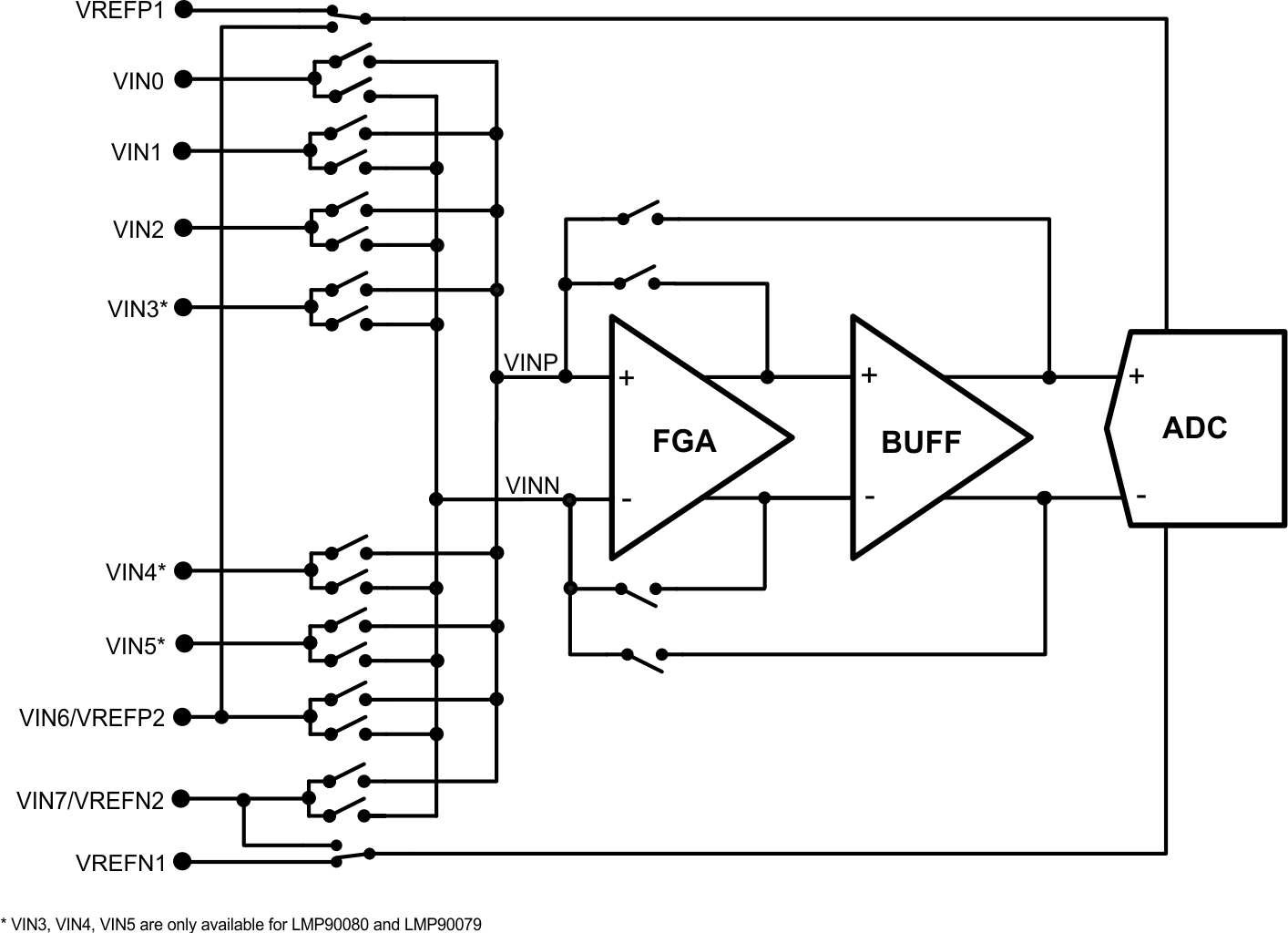 Figure 43. Simplified VIN Circuitry
9.3.7.3 Selectable Gains (FGA and PGA)
LMP900xx provides two types of gain amplifiers: a fixed gain amplifier (FGA) and a programmable gain amplifier (PGA). FGA has a fixed gain of 16x or it can be bypassed, while the PGA has programmable gain settings of 1x, 2x, 4x, or 8x.
Total gain is defined as FGA x PGA. Thus, LMP900xx provides gain settings of 1x, 2x, 4x, 8x, 16x, 32x, 64x, or 128x with true continuous background calibration.
The gain is channel specific, which means that one channel can have one gain, while another channel can have the same or a different gain.
The gain can be selected by programming the CHx_CONFIG: GAIN_SEL bits.
9.3.7.4 Buffer (BUFF)
There is an internal unity gain buffer that can be included or excluded from the signal path. Including the buffer provides a high input impedance but increases the power consumption.
When gain ≥ 16, the buffer is automatically included in the signal path. When gain < 16, including or excluding the buffer from the signal path can be done by programming the CHX_CONFIG: BUF_EN bit.
9.3.7.5 Internal/External CLK Selection
LMP900xx allows two clock options: internal CLK or external CLK (crystal (XTAL) or clock source).
There is an “External Clock Detection” mode, which detects the external XTAL if it is connected to XOUT and XIN. When operating in this mode, the LMP900xx shuts off the internal clock to reduce power consumption. Below is a flow chart to help set the appropriate clock registers.
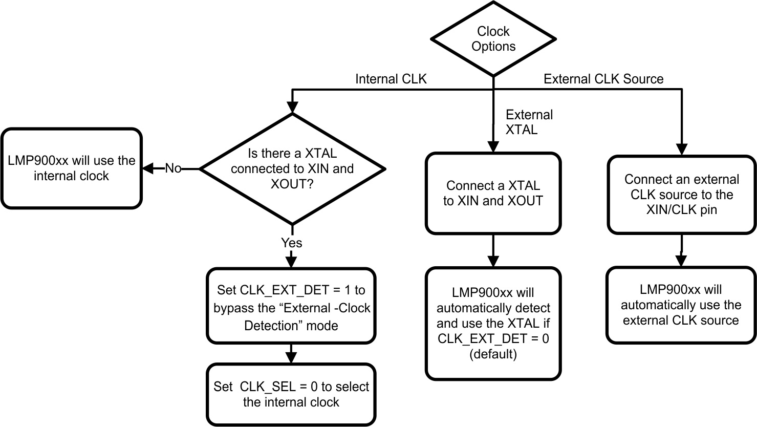 Figure 44. CLK Register Settings
The recommended value for the external CLK is discussed in the next sections.
9.3.7.6 Programmable ODRS
If using the internal CLK or external CLK of 3.5717 MHz, then the output date rates (ODR) can be selected (using the ODR_SEL bit) as:
1. 13.42/8 = 1.6775 SPS
2. 13.42/4 = 3.355 SPS
3. 13.42/2 = 6.71SPS
4. 13.42 SPS
5. 214.65/8 = 26.83125 SPS
6. 214.65/4 = 53.6625 SPS
7. 214.65/2 = 107.325 SPS
8. 214.65 SPS (default)
If the internal CLK is not being used and the external CLK is not 3.5717 MHz, then the ODR will be different. If this is the case, use the equation below to calculate the new ODR values.
For example, a 3.6864 MHz XTAL or external clock has the following ODR values:
The ODR is channel specific, which means that one channel can have one ODR, while another channel can have the same or a different ODR.
Note that these ODRs are meant for a single channel conversion; the ODR needs to be divided by n for n channels scanning. For example, if the ADC were running at 214.65 SPS and four channels are being scanned, then the ODR per channel would be 214.65/4 = 53.6625 SPS.
9.3.7.7 Digital Filter
The LMP900xx has a fourth order rotated sinc filter that is used to configure various ODRs and to reject power supply frequencies of 50Hz and 60Hz. The 50/60 Hz rejection is only effective when the device is operating at ODR ≤ 13.42 SPS. If the internal CLK or the external CLK of 3.5717 MHz is used, then the LMP900xx will have the frequency response shown in Figure 45 through Figure 49.
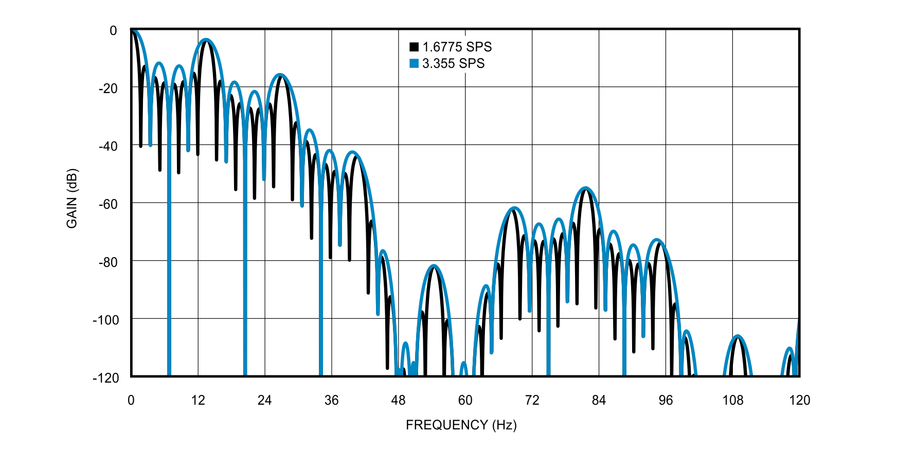 Figure 45. Digital Filter Response, 1.6775 SPS and 3.355 SPS
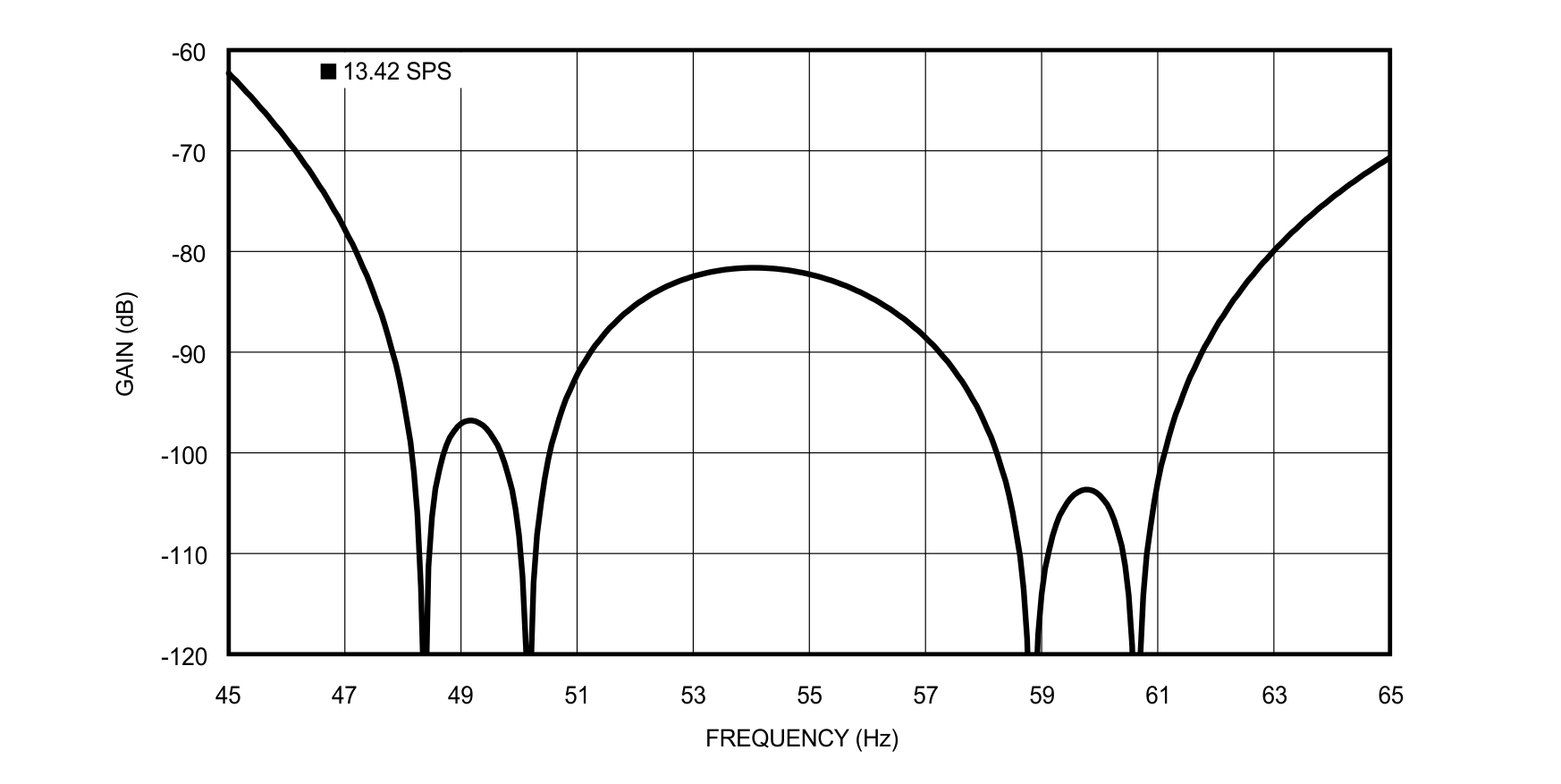 Figure 47. Digital Filter Response at 13.42 SPS
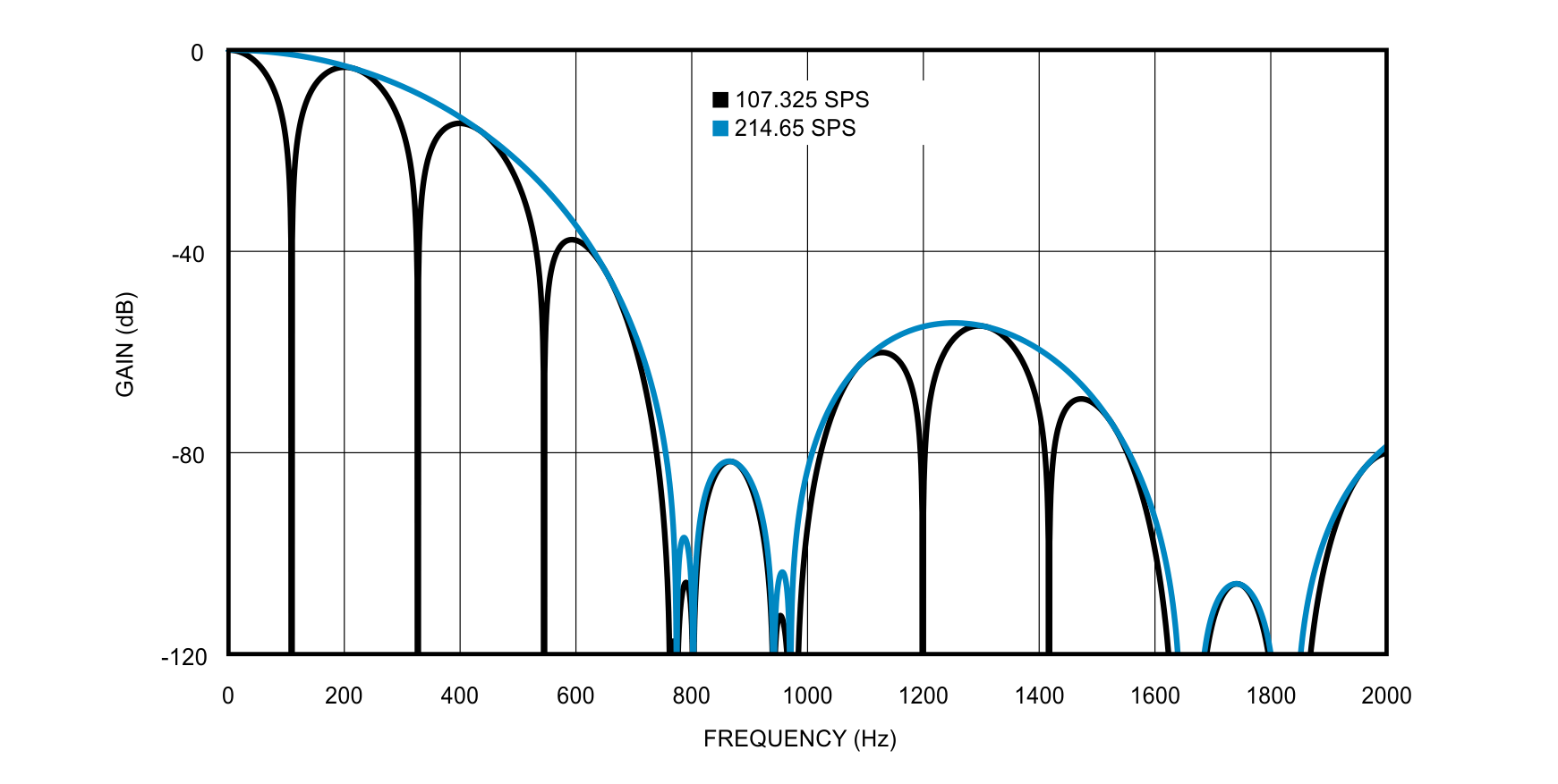 Figure 49. Digital Filter Response 107.325 SPS and 214.65 SPS
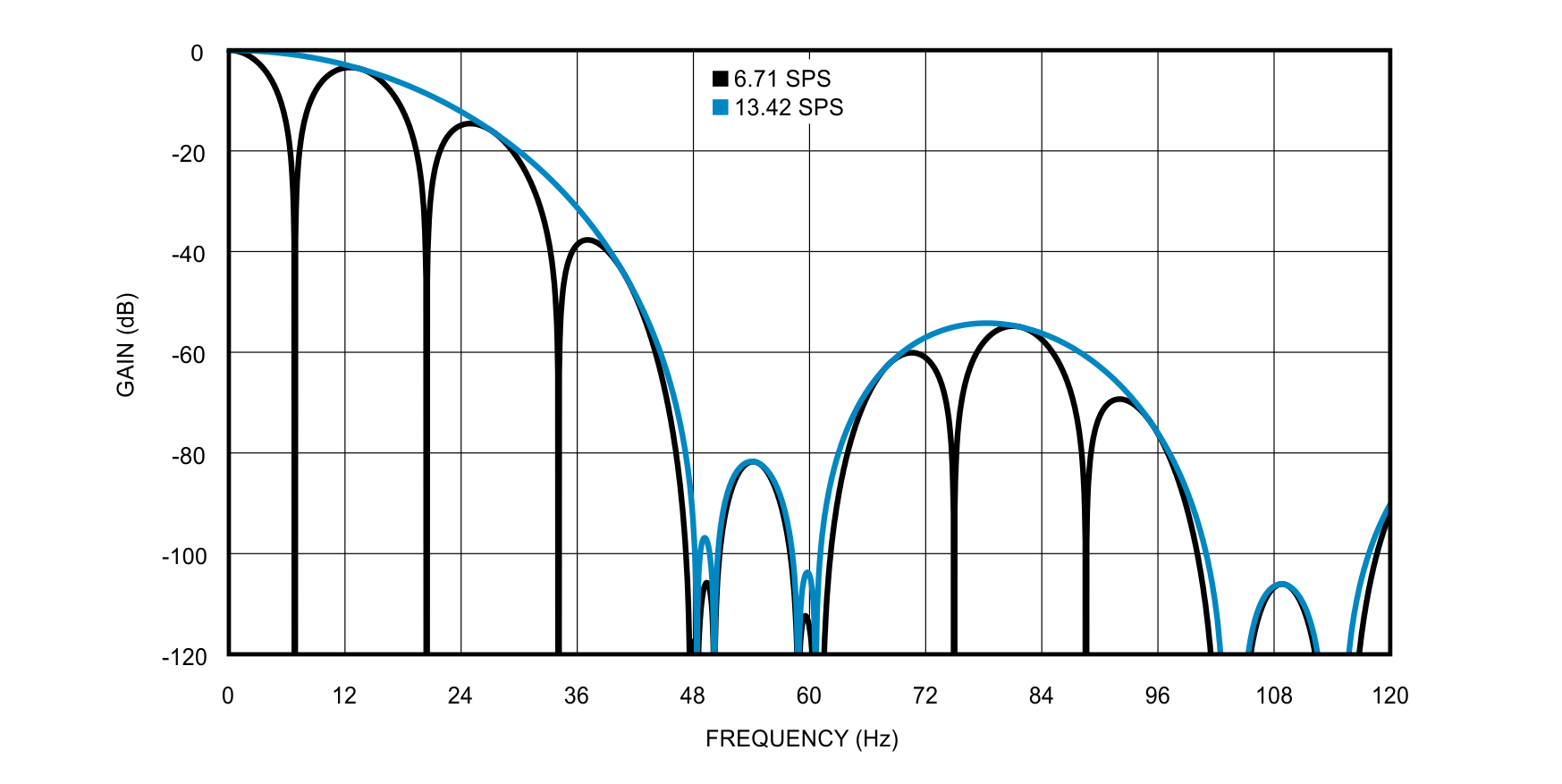 Figure 46. Digital Filter Response, 6.71 SPS and 13.42 SPS
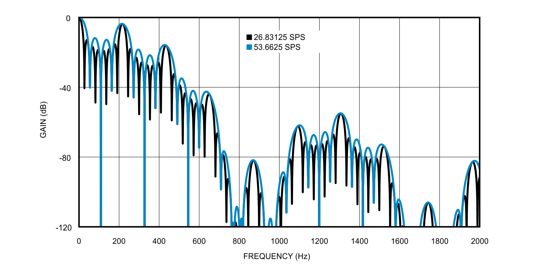 Figure 48. Digital Filter Response, 26.83125 SPS and 53.6625 SPS
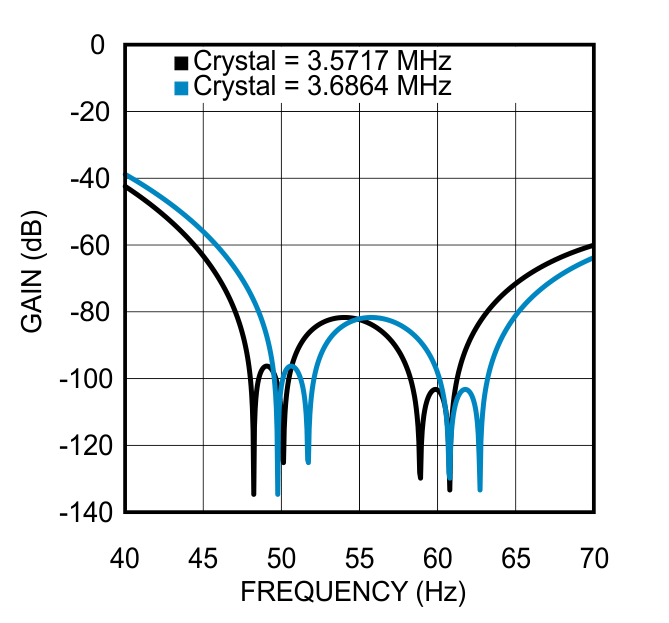 Figure 50. Digital Filter Response for a 3.5717 MHz Versus 3.6864 MHz XTAL
If the internal CLK is not being used and the external CLK is not 3.5717 MHz, then the filter response would be the same as the response shown above, but the frequency will change according to the equation:
Using Equation 9, an example of the filter response for a 3.5717 MHz XTAL versus a 3.6864 MHz XTAL can be seen in Figure 50.
9.3.7.8 GPIO (D0–D6)
Pins D0-D6 are general purpose input/output (GPIO) pins that can be used to control external LEDs or switches. Only a high or low value can be sourced to or read from each pin.
Figure 51 shows a flowchart how these GPIOs can be programmed.
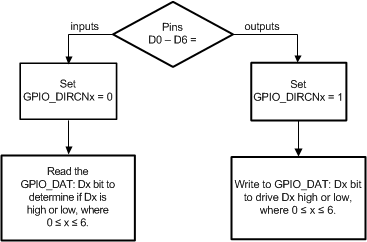 Figure 51. GPIO Register Settings
9.4 Device Functional Modes
9.4.1 Channels Scan Mode
There are four scan modes. These scan modes are selected using the CH_SCAN: CH_SCAN_SEL bit. The first scanned channel is FIRST_CH, and the last scanned channel is LAST_CH; they are both located in the CH_SCAN register.
The CH_SCAN register is double buffered. That is, user inputs are stored in a slave buffer until the start of the next conversion during which time they are transferred to the master buffer. Once the slave buffer is written, subsequent updates are disregarded until a transfer to the master buffer happens. Hence, it may be appropriate to check the CH_SCAN_NRDY bit before programming the CH_SCAN register.
9.4.1.1 ScanMode0: Single-Channel Continuous Conversion
LMP900xx continuously converts the selected FIRST_CH.
Do not operate in this scan mode if gain ≥ 16 and the LMP900xx is running in background calibration modes BgcalMode1 or BgcalMode2. If this is the case, then it is more suitable to operate the device in ScanMode2 instead.
9.4.1.2 ScanMode1: Multiple-Channels Single Scan
LMP900xx converts one or more channels starting from FIRST_CH to LAST_CH, and then enters the stand-by state.
9.4.1.3 ScanMode2: Multiple-Channels Continuous Scan
LMP900xx continuously converts one or more channels starting from FIRST_CH to LAST_CH, and then it repeats this process.
9.4.1.4 ScanMode3: Multiple-Channels Continuous Scan with Burnout Currents
This mode is the same as ScanMode2 except that the burnout current is provided in a serially scanned fashion (injected in a channel after it has undergone a conversion). Thus it avoids burnout current injection from interfering with the conversion result for the channel.
The sensor diagnostic burnout currents are available for all four scan modes. The burnout current is further gated by the BURNOUT_EN bit for each channel. ScanMode3 is the only mode that scans multiple channels while injecting burnout currents without interfering with the signal. This is described in details in Burnout Currents.
9.4.2 Sensor Interface
The LMP90080/LMP90078 contains two excitation currents (IB1 & IB2) for sourcing external sensors, and the LMP900xx contain two burnout currents for sensor diagnostics. They are described in the next sections.
9.4.2.1 IB1 & IB2 - Excitation Currents (LMP90080/LMP90078)
IB1 and IB2 can be used for providing currents to external sensors, such as RTDs or bridge sensors. 100µA to 1000µA, in steps of 100µA, can be sourced by programming the ADC_AUXCN: RTD_CUR_SEL bits.
Refer to 3–Wire RTD to see how IB1 and IB2 can be used to source a 3-wire RTD.
9.4.2.2 Burnout Currents
As shown in Figure 52, the LMP900xx contains two internal 10 µA burnout current sources, one sourcing current from VA to VINP, and the other sinking current from VINN to ground. These currents are used for sensor diagnostics and can be enabled for each channel using the CHx_INPUTCN: BURNOUT_EN bit.
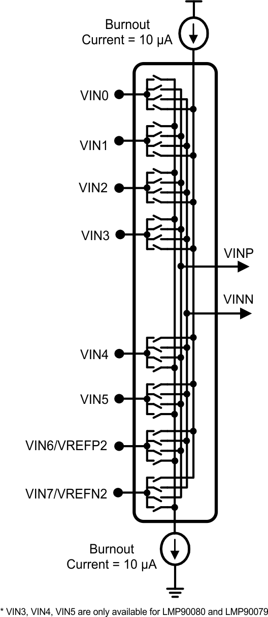 Figure 52. Burnout Currents
9.4.2.2.1 Burnout Current Injection
Burnout currents are injected differently depending on the channel scan mode selected.
When BURNOUT_EN = 1 and the device is operating in ScanMode0, 1, or 2, the burnout currents are injected into all the channels for which the BURNOUT_EN bit is selected. This will cause problems and hence in this mode, more than one channel should not have its BURNOUT_EN bit selected. Also, the burnout current will interfere with the signal and introduce a fixed error depending on the particular external sensor.
When BURNOUT_EN = 1 and the device is operating in ScanMode3, burnout currents are injected into the last sampled channel on a cyclical basis (Figure 53). In this mode, burnout currents injection is truly done in the background without affecting the accuracy of the on-going conversion. Operating in this mode is recommended.
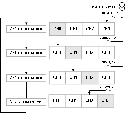 Figure 53. Burnout Currents Injection for Scanmode3
9.4.2.3 Sensor Diagnostic Flags
Burnout currents can be used to verify that an external sensor is still operational before attempting to make measurements on that channel. A non-operational sensor means that there is a possibility the connection between the sensor and the LMP900xx is open circuited, short circuited, shorted to VA or GND, overloaded, or the reference may be absent. The sensor diagnostic flags diagram can be seen in Figure 54.
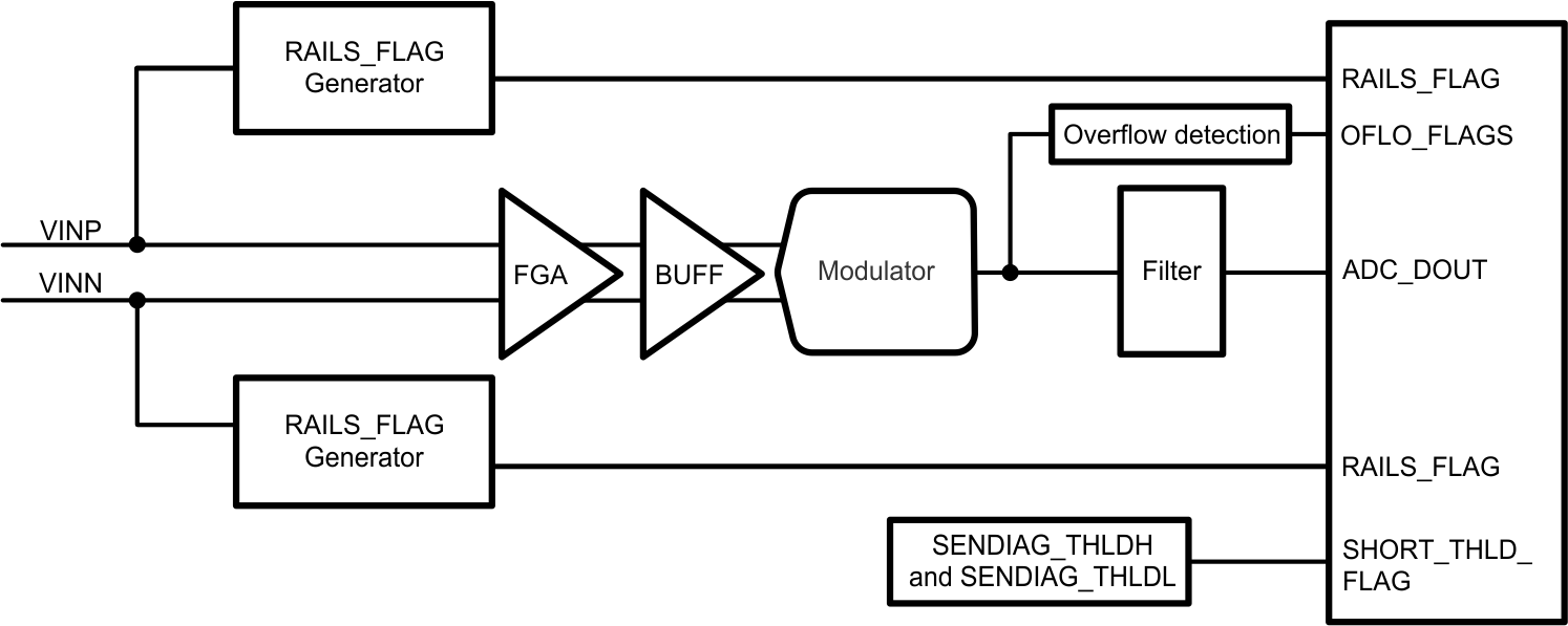 Figure 54. Sensor Diagnostic Flags Diagram
The sensor diagnostic flags are located in the SENDIAG_FLAGS register and are described in further details below.
9.4.2.3.1 SHORT_THLD_FLAG
The short circuit threshold flag is used to report a short-circuit condition. It is set when the output voltage (VOUT) is within the absolute Vthreshold. Vthreshold can be programmed using the 8-bit SENDIAG_THLDH register.
For example, assume VREF = 5V, gain = 1, SENDIAG_THLD = 0xDA (218d). In this case, Vthreshold can be calculated as:
When (-33.3mV) ≤ VOUT ≤ (33.3mV), then SHORT_THLD_FLAG = 1; otherwise, SHORT_THLD_FLAG = 0.
9.4.2.3.2 RAILS_FLAG
The rails flag is used to detect if one of the sampled channels is within 50mV of the rails potential (VA or VSS). This can be further investigated to detect an open-circuit or short-circuit condition. If the sampled channel is near a rail, then RAILS_FLAG = 1; otherwise, RAILS_FLAG = 0.
9.4.2.3.3 POR_AFT_LST_RD
If POR_AFT_LST_READ = 1, then there was a power-on reset since the last time the SENDIAG_FLAGS register was read. This flag's status is cleared when this bit is read, unless this bit is set again on account of another power-on-reset event in the intervening period.
9.4.2.3.4 OFLO_FLAGS
OFLO_FLAGS is used to indicate whether the modulator is over-ranged or under-ranged. The following conditions are possible:
- OFLO_FLAGS = 0x0: Normal Operation
- OFLO_FLAGS = 0x1: The differential input is more than (±VREF/Gain) but is not more than ±(1.3*VREF/Gain) to cause a modulator over-range.
- OFLO_FLAGS = 0x2: The modulator was over-ranged towards +VREF/Gain.
- OFLO_FLAGS = 0x3: The modulator was over-ranged towards −VREF/Gain.
The condition of OFLO_FLAGS = 10b or 11b can be used in conjunction with the RAILS_FLAG to determine the fault condition.
9.4.2.3.5 SAMPLED_CH
These three bits show the channel number for which the ADC_DOUT and SENDIAG_FLAGS are available. This does not necessarily indicate the current channel under conversion because the conversion frame and computation of results from the channels are pipelined. That is, while the conversion is going on for a particular channel, the results for the previous conversion (of the same or a different channel) are available.
9.5 Programming
9.5.1 Serial Digital Interface
A synchronous 4-wire serial peripheral interface (SPI) provides access to the internal registers of LMP900xx via CSB, SCLK, SDI, SDO/DRDYB.
9.5.1.1 Register Address (ADDR)
All registers are memory-mapped. A register address (ADDR) is composed of an upper register address (URA) and lower register address (LRA) as shown in Table 5. For example, ADDR 0x3A has URA=0x3 and LRA=0xA.
Table 5. ADDR Map
| BIT | [6:4] | [3:0] |
|---|---|---|
| Name | URA | LRA |
9.5.1.2 Register Read/Write Protocol
Figure 55 shows the protocol how to write to or read from a register.
Transaction 1 sets up the upper register address (URA) where the user wants to start the register-write or register-read.
Transaction 2 sets the lower register address (LRA) and includes the Data Byte(s), which contains the incoming data from the master or outgoing data from the LMP900xx.
Examples of register-reads or register-writes can be found in Register Read/Write Examples.
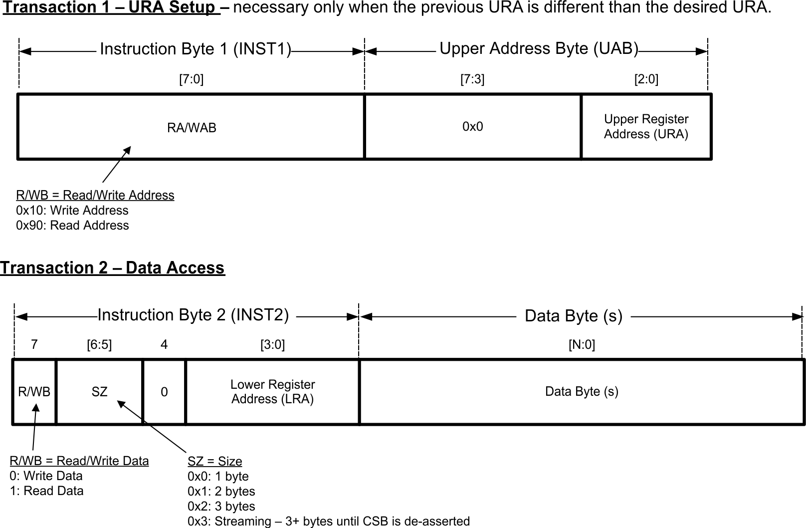 Figure 55. Register Read/Write Protocol
9.5.1.3 Streaming
When writing/reading 3+ bytes, the user must operate the device in Normal Streaming mode or Controlled Streaming mode. In the Normal Streaming mode, which is the default mode, data runs continuously starting from ADDR until CSB deasserts. This mode is especially useful when programming all the configuration registers in a single transaction. See the Normal Streaming Example section for an example of the Normal Streaming mode.
In the Controlled Streaming mode, data runs continuously starting from ADDR until the data has run through all (STRM_RANGE + 1) registers. For example, if the starting ADDR is 0x1C, STRM_RANGE = 5, then data will be written to or read from the following ADDRs: 0x1C, 0x1D, 0x1E, 0x1F, 0x20, 0x21. Once the data reaches ADDR 0x21, LMP900xx will wrap back to ADDR 0x1C and repeat this process until CSB deasserts. See the Controlled Streaming Example section for an example of the Controlled Streaming mode.
If streaming reaches ADDR 0x7F, then it will wrap back to ADDR 0x00. Furthermore, reading back the Upper Register Address after streaming will report the Upper Register Address at the start of streaming, not the Upper Register Address at the end of streaming.
To stream, write 0x3 to INST2’s SZ bits as seen in Figure 55. To select the stream type, program the SPI_STREAMCN: STRM_TYPE bit. The STRM_RANGE can also be programmed in the same register.
9.5.1.4 CSB – Chip Select Bar
An SPI transaction begins when the master asserts (active low) CSB and ends when the master deasserts (active high) CSB. Each transaction might be separated by a subsequent one with a CSB deassertion, but this is optional. Once CSB is asserted, it must not pulse (deassert and assert again) during a (desired) transaction.
CSB can be grounded in systems where LMP900xx is the only SPI slave. This frees the software from handling the CSB. Care has to be taken to avoid any false edge on SCLK, and while operating in this mode, the streaming transaction should not be used because exiting from this mode can only be done through a CSB deassertion.
9.5.1.5 SPI Reset
SPI Reset resets the SPI-Protocol State Machine by monitoring the SDI for at least 73 consecutive 1's at each SCLK rising edge. After an SPI Reset, SDI is monitored for a possible Write Instruction at each SCLK rising edge.
SPI Reset will reset the Upper Address Register (URA) to 0, but the register contents are not reset.
By default, SPI reset is disabled, but it can be enabled by writing 0x01 to SPI Reset Register (ADDR 0x02).
9.5.1.6 DRDYB - Data Ready Bar
DRDYB is a signal generated by the LMP900xx that indicates a fresh conversion data is available in the ADC_DOUT registers.
DRDYB is automatically asserted every (1/ODR) second as seen in Figure 56. Before the next assertion, DRDYB will pulse for tDRDYB second. The value for tDRDYB can be found in Timing Requirements.
 Figure 56. DRDYB Behavior
If ADC_DOUT is being read while a new ADC_DOUT becomes available, then the ADC_DOUT that is being read is still valid (Figure 57). DRDYB will still be deasserted every 1/ODR second, but a consecutive read on the ADC_DOUT register will fetch the newly converted data available.
 Figure 57. DRDYB Behavior For An Incomplete ADC_DOUT Reading
DRDYB can also be accessed via registers using the DT_AVAIL_B bit. This bit indicates when fresh conversion data is available in the ADC_DOUT registers. If new conversion data is available, then DT_AVAIL_B = 0; otherwise, DT_AVAIL_B = 1.
A complete reading for DT_AVAIL_B occurs when the MSB of ADC_DOUTH is read out. This bit cannot be reset even if REG_AND_CNV_RST = 0xC3.
9.5.1.6.1 DrdybCase1: Combining SDO/DRDYB with SDO_DRDYB_DRIVER = 0x00
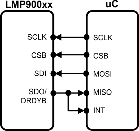 Figure 58. DrdybCase1 Connection Diagram
As shown in Figure 58, the DRDYB signal and SDO can be multiplexed on the same pin as their functions are mostly complementary. In fact, this is the default mode for the SDO/DRDYB pin.
Figure 59 shows a timing protocol for DrdybCase1. In this case, start by asserting CSB first to monitor a DRDYB assertion. When the DRDYB signal asserts, begin writing the Instruction Bytes (INST1, UAB, INST2) to read from or write to registers. Note that INST1 and UAB are omitted from the figure below because this transaction is only required if a new UAB needs to be implemented.
While the CSB is asserted, DRDYB is driving the SDO/DRDYB pin unless the device is reading data, in which case, SDO will be driving the pin. If CSB is deasserted, then the SDO/DRDYB pin is High-Z.
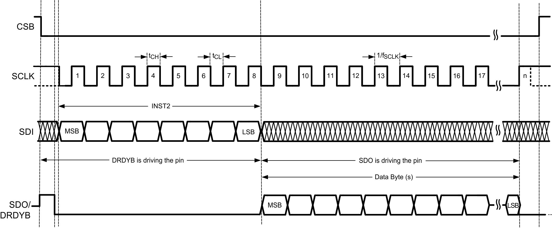 Figure 59. Timing Protocol for DrdybCase1
9.5.1.6.2 DrdybCase2: Combining SDO/DRDYB with SDO_DRDYB_DRIVER = 0x03
SDO/DRDYB can be made independent of CSB by setting SDO_DRDYB_DRIVER = 0x03 in the SPI Handshake Control register. In this case, DRDYB will drive the pin unless the device is reading data, independent of the state of CSB. SDO will drive the pin when CSB is asserted and the device is reading data.
With this scheme, one can use SDO/DRDYB as a true interrupt source, independent of the state of CSB. But this scheme can only be used when the LMP900xx is the only device connected to the master's SPI bus because the SDO/DRDYB pin will be DRDYB even when CSB is deasserted.
The timing protocol for this case can be seen in Figure 60. When DRDYB asserts, assert CSB to start the SPI transaction and begin writing the Instruction Bytes (INST1, UAB, INST2) to read from or write to registers.
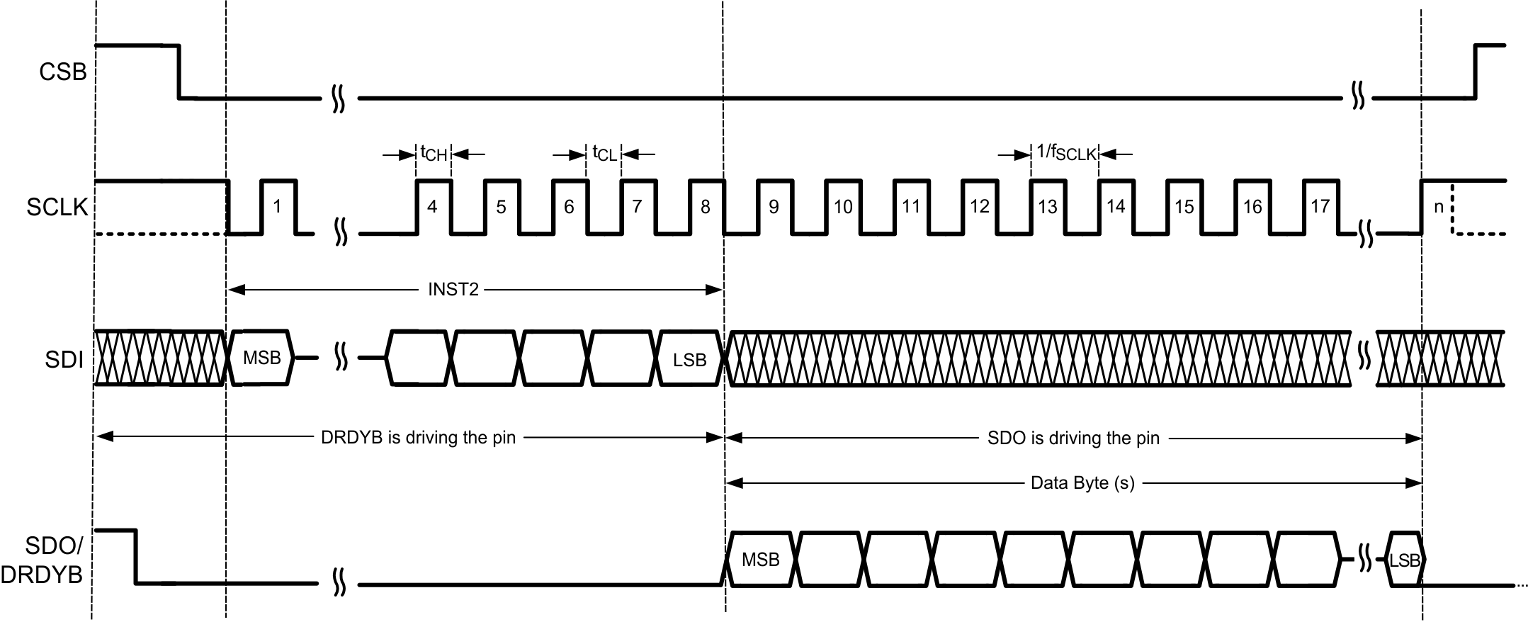 Figure 60. Timing Protocol For DrdybCase2
9.5.1.6.3 DrdybCase3: Routing DRDYB to D6
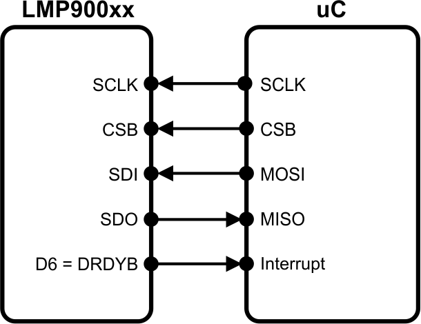 Figure 61. DrdybCase3 Connection Diagram
The DRDYB signal can be routed to pin D6 by setting SPI_DRDYB_D6 high and SDO_DRDYB_DRIVER to 0x4. This is the behavior for DrdybCase3 as shown in Figure 61.
The timing protocol for this case can be seen in Figure 62. Since DRDYB is separated from SDO, it can be monitored using the interrupt or polling method. If polled, the DRDYB signal needs to be polled faster than tDRDYB to detect a DRDYB assertion. When DRDYB asserts, assert CSB to start the SPI transaction and begin writing the Instruction Bytes (INST1, UAB, INST2) to read from or write to registers.
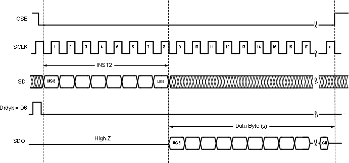 Figure 62. Timing Protocol for DrdybCase3
9.5.1.7 Data Only Read Transaction
In a data only read transaction, one can directly access the data byte(s) as soon as the CSB is asserted without having to send any instruction byte. This is useful as it brings down the latency as well as the overhead associated with the instruction byte (as well as the Upper Address Byte, if any).
In order to use the data only transaction, the device must be placed in the data first mode. The following table lists transaction formats for placing the device in and out of the data first mode and reading the mode status.
Table 6. Data First Mode Transactions
| BIT[7] | BITS[6:5] | BIT[4] | BITS[3:0] | DATA BYTES | |
|---|---|---|---|---|---|
| Enable Data First Mode Instruction | 1 | 11 | 1 | 1010 | None |
| Disable Data First Mode Instruction | 1 | 11 | 1 | 1011 | None |
| Read Mode Status Transaction | 1 | 00 | 1 | 1111 | One |
Note that while being in the data first mode, once the data bytes in the data only read transaction are sent out, the device is ready to start on any normal (non-data-only) transaction including the Disable Data First Mode Instruction. The current status of the data first mode (enabled/disabled status) can be read back using the Read Mode Status Transaction. This transaction consists of the Read Mode Status Instruction followed by a single data byte (driven by the device). The data first mode status is available on bit [1] of this data byte.
The data only read transaction allows reading up to eight consecutive registers, starting from any start address. Usually, the start address will be the address of the most significant byte of conversion data, but it could just as well be any other address. The start address and number of bytes to be read during the data only read transaction can be programmed using the DATA_ONLY_1 AND DATA_ONLY_2 registers respectively.
The upper register address is unaffected by a data only read transaction. That is, it retains its setting even after encountering a data only transaction. The data only transaction uses its own address (including the upper address) from the DATA_ONLY_1 register. When in the data first mode, the SCLK must stop high before entering the Data Only Read Transaction; this transaction should be completed before the next scheduled DRDYB deassertion.
9.5.1.8 Cyclic Redundancy Check (CRC)
CRC can be used to ensure integrity of data read from LMP900xx. To enable CRC, set EN_CRC high. Once CRC is enabled, the CRC value is calculated and stored in SPI_CRC_DAT so that the master device can periodically read for data comparison. The CRC is automatically reset when CSB or DRDYB is deasserted.
The CRC polynomial is x8 + x5 + x4 + 1. The reset value of the SPI_CRC_DAT register is zero, and the final value is ones-complemented before it is sent out. Note that CRC computation only includes the bits sent out on SDO and does not include the bits of the SPI_CRC_DAT itself; thus it is okay to read SPI_CRC_DAT repeatedly.
The DRDYB signal normally deasserts (active high) every 1/ODR second. However, this behavior can be changed so that DRDYB deassertion can occur after SPI_CRC_DAT is read, but not later than normal DRDYB deassertion which occurs at every 1/ODR seconds. This is done by setting bit DRDYB_AFT_CRC high.
The timing protocol for CRC can be found in Figure 63.
 Figure 63. Timing Protocol for Reading SPI_CRC_DAT
If SPI_CRC_DAT read extends beyond the normal DRDYB deassertion at every 1/ODR seconds, then CRC_RST has to be set in the SPI Data Ready Bar Control Register. This is done to avoid a CRC reset at the DRDYB deassertion. Timing protocol for reading CRC with CRC_RST set is shown in Figure 64.
 Figure 64. Timing Protocol for Reading SPI_CRC_DAT Beyond Normal DRDYB Deassertion at Every 1/ODR Seconds
Follow the steps below to enable CRC:
9.5.2 RESET and RESTART
Writing 0xC3 to the REG_AND_CNV_RST field will reset the conversion and most of the programmable registers to their default values. The only registers that will not be reset are the System Calibration Registers (CHx_SCAL_OFFSET, CHx_SCAL_GAIN) and the DT_AVAIL_B bit.
If it is desirable to reset the System Calibration Coefficient Registers, then set RESET_SYSCAL = 1 before writing 0xC3 to REG_AND_CNV_RST. If the device is operating in the “System Calibration Offset/Gain Coefficient Determination” mode (SCALCN register), then write REG_AND_CNV_RST = 0xC3 twice to get out of this mode.
After a register reset, any on-going conversions will be aborted and restarted. If the device is in the power-down state, then a register reset will bring it out of the power-down state.
To restart a conversion, write 1 to the RESTART bit. This bit can be used to synchronize the conversion to an external event.
After a restart conversion, the first sample is not valid. To restart with a valid first sample, issue a stand-by command followed by an active command.
9.5.3 Register Read/Write Examples
9.5.3.1 Writing to Register Examples
Using the register read/write protocol shown in Figure 55, the following example shows how to write three data bytes starting at register address (ADDR) 0x1F. After the last byte has been written to ADDR 0x21, deassert CSB to end the register-write.
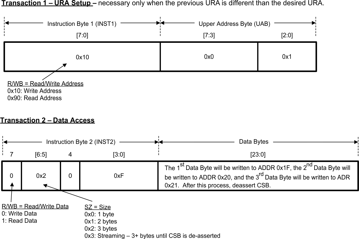 Figure 65. Register-Write Example 1
The next example shows how to write one data byte to ADDR 0x12. Since the URA for this example is the same as the last example, transaction 1 can be omitted.
 Figure 66. Register-Write Example 2
9.5.3.2 Reading from Register Example
The following example shows how to read two bytes. The first byte will be read from starting ADDR 0x24, and the second byte will be read from ADDR 0x25.
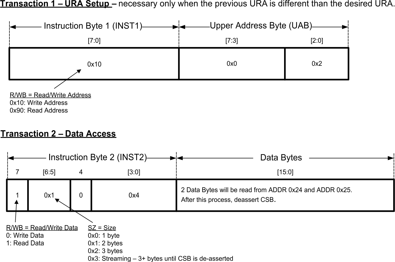 Figure 67. Register-Read Example
9.5.4 Streaming Examples
9.5.4.1 Normal Streaming Example
This example shows how to write six data bytes starting at ADDR 0x28 using the Normal Streaming mode. Because the default STRM_TYPE is the Normal Streaming mode, setting up the SPI_STREAMCN register can be omitted.
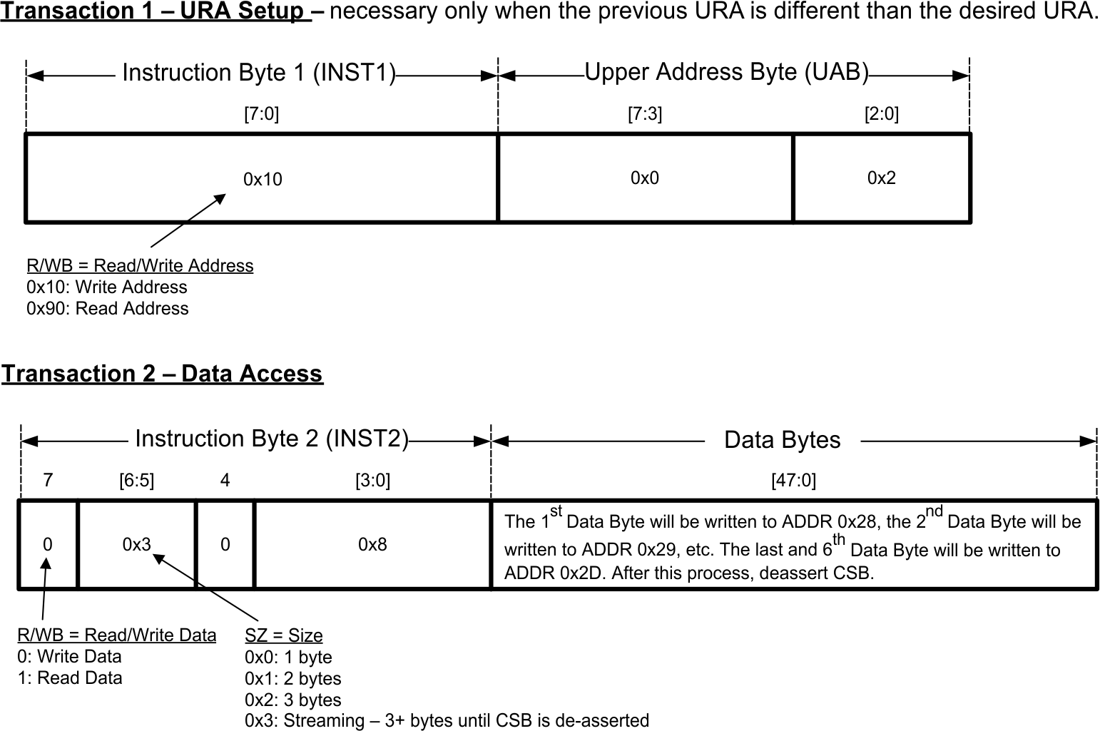 Figure 68. Normal Streaming Example
9.5.4.2 Controlled Streaming Example
This example shows how to read the 16-bit conversion data (ADC_DOUT) four times using the Controlled Streaming mode. The ADC_DOUT registers consist of ADC_DOUTH at ADDR 0x1A and ADC_DOUTL at ADDR 0x1B.
The first step (Figure 69) sets up the SPI_STREAMCN register. This step enters the Controlled Streaming mode by setting STRM_TYPE high in ADDR 0x03. Since two registers (ADDR 0x1A - 0x1B) need to be read, the STRM_RANGE is 1.
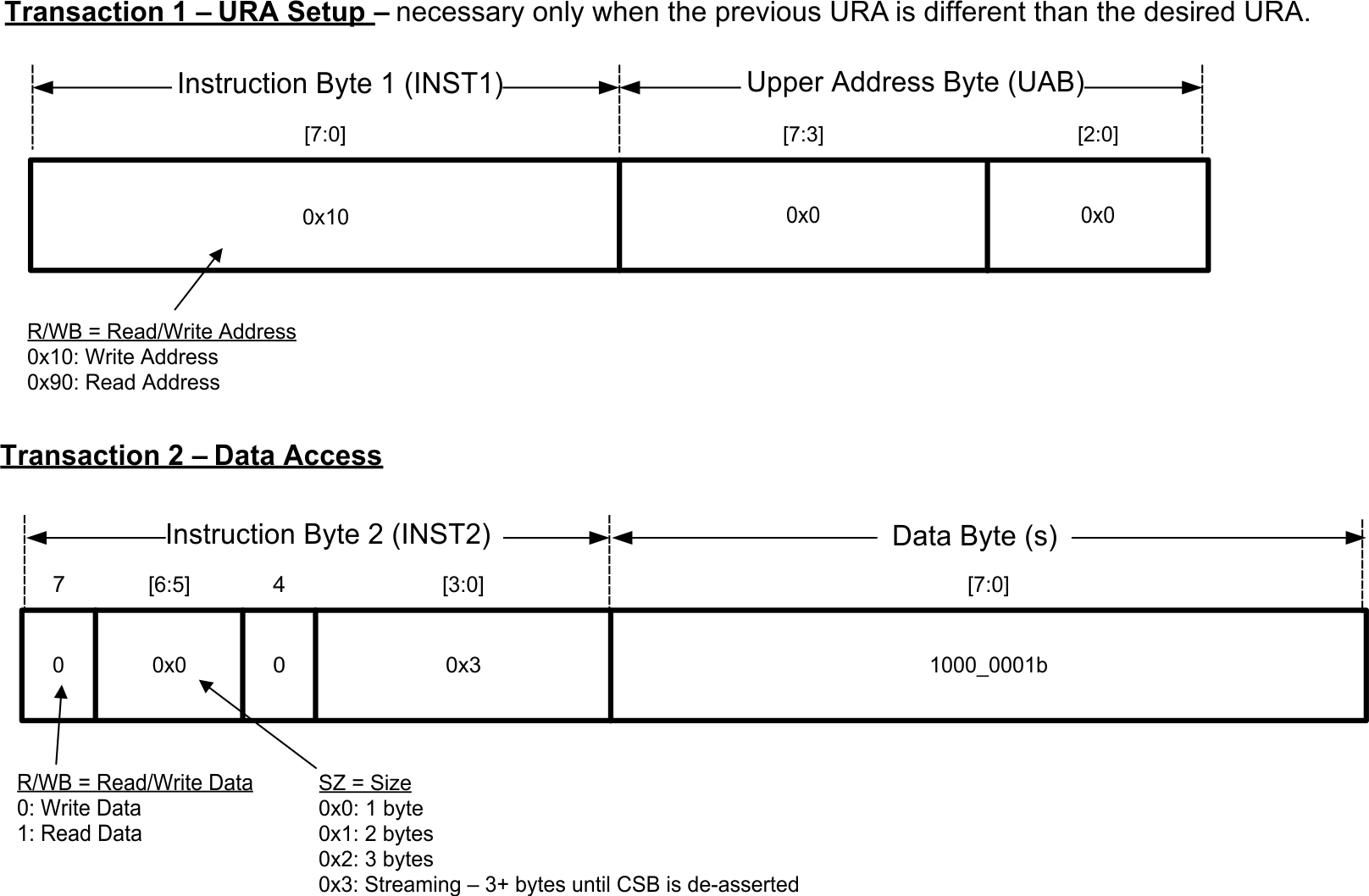 Figure 69. Setting Up SPI_STREAMCN
The next step shows how to perform the Controlled Streaming mode so that the master device will read ADC_DOUT from ADDR 0x1A and 0x1B, then wrap back to ADDR 0x1A, and repeat this process for four times. After this process, deassert CSB to end the Controlled Streaming mode.
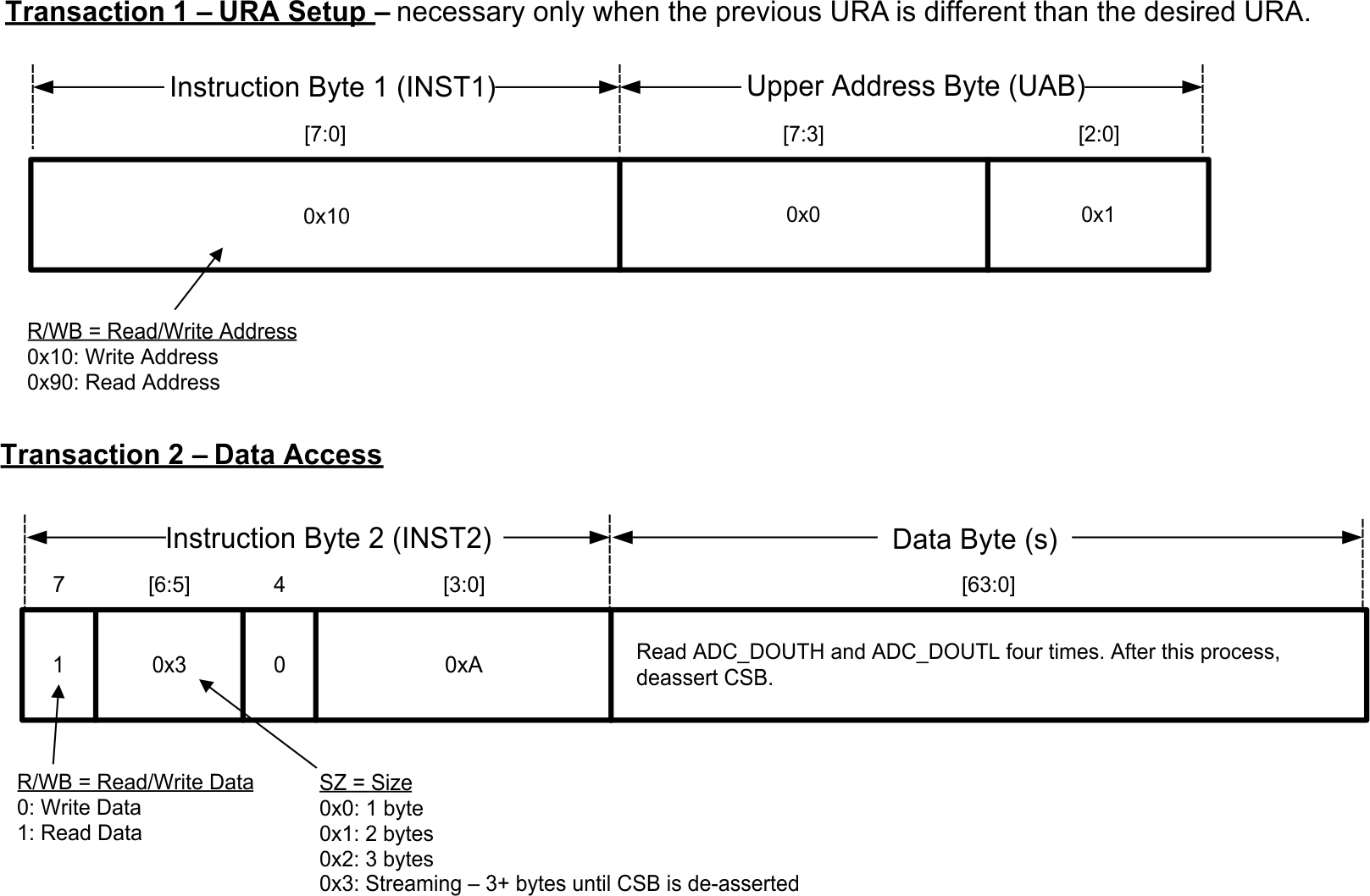 Figure 70. Controlled Streaming Example
9.6 Register Maps
- If written to, RESERVED bits must be written to only 0 unless otherwise indicated.
- Read back value of RESERVED bits and registers is unspecified and should be discarded.
- Recommended values must be programmed and forbidden values must not be programmed where they are indicated in order to avoid unexpected results.
- If written to, registers indicated as Reserved must have the indicated default value as shown below. Any other value can cause unexpected results.
Table 7. Register Map
| REGISTER NAME | ADDR (URA & LRA) | TYPE | DEFAULT | |
|---|---|---|---|---|
| RESETCN | Reset Control | 0x00 | WO | - |
| SPI_HANDSHAKECN | SPI Handshake Control | 0x01 | R/W | 0x00 |
| SPI_RESET | SPI Reset Control | 0x02 | R/W | 0x00 |
| SPI_STREAMCN | SPI Stream Control | 0x03 | R/W | 0x00 |
| Reserved | - | 0x04 - 0x07 | - | 0x00 |
| PWRCN | Power Mode Control and Status | 0x08 | RO & WO | 0x00 |
| DATA_ONLY_1 | Data Only Read Control 1 | 0x09 | R/W | 0x1A |
| DATA_ONLY_2 | Data Only Read Control 2 | 0x0A | R/W | 0x02 |
| ADC_RESTART | ADC Restart Conversion | 0x0B | WO | - |
| Reserved | - | 0x0C - 0x0D | - | 0x00 |
| GPIO_DIRCN | GPIO Direction Control | 0x0E | R/W | 0x00 |
| GPIO_DAT | GPIO Data | 0x0F | RO & WO | - |
| BGCALCN | Background Calibration Control | 0x10 | R/W | 0x00 |
| SPI_DRDYBCN | SPI Data Ready Bar Control | 0x11 | R/W | 0x03 |
| ADC_AUXCN | ADC Auxiliary Control | 0x12 | R/W | 0x00 |
| SPI_CRC_CN | CRC Control | 0x13 | R/W | 0x02 |
| SENDIAG_THLD | Sensor Diagnostic Threshold | 0x14 | R/W | 0x00 |
| Reserved | - | 0x15-0x16 | - | 0x0000 |
| SCALCN | System Calibration Control | 0x17 | R/W | 0x00 |
| ADC_DONE | ADC Data Available | 0x18 | RO | - |
| SENDIAG_FLAGS | Sensor Diagnostic Flags | 0x19 | RO | - |
| ADC_DOUT | Conversion Data 1 and 0 | 0x1A - 0x1B | RO | - |
| Reserved | - | 0x1C | - | - |
| SPI_CRC_DAT | CRC Data | 0x1D | RO & WO | - |
| CHANNEL CONFIGURATION REGISTERS (CH4 to CH6 for LMP90080/LMP90079 only) | ||||
| CH_STS | Channel Status | 0x1E | RO | 0x00 |
| CH_SCAN | Channel Scan Mode | 0x1F | R/W | 0x30 |
| CH0_INPUTCN | CH0 Input Control | 0x20 | R/W | 0x01 |
| CH0_CONFIG | CH0 Configuration | 0x21 | R/W | 0x70 |
| CH1_INPUTCN | CH1 Input Control | 0X22 | R/W | 0x13 |
| CH1_CONFIG | CH1 Configuration | 0x23 | R/W | 0x70 |
| CH2_INPUTCN | CH2 Input Control | 0x24 | R/W | 0x25 |
| CH2_CONFIG | CH2 Configuration | 0x25 | R/W | 0x70 |
| CH3_INPUTCN | CH3 Input Control | 0x26 | R/W | 0x37 |
| CH3_CONFIG | CH3 Configuration | 0x27 | R/W | 0x70 |
| CH4_INPUTCN | CH4 Input Control | 0x28 | R/W | 0x01 |
| CH4_CONFIG | CH4 Configuration | 0x29 | R/W | 0x70 |
| CH5_INPUTCN | CH5 Input Control | 0x2A | R/W | 0x13 |
| CH5_CONFIG | CH5 Configuration | 0x2B | R/W | 0x70 |
| CH6_INPUTCN | CH6 Input Control | 0x2C | R/W | 0x25 |
| CH6_CONFIG | CH6 Configuration | 0x2D | R/W | 0x70 |
| Reserved | - | 0x2E - 0x2F | - | 0x00 |
| SYSTEM CALIBRATION REGISTERS | ||||
| CH0_SCAL_OFFSET | CH0 System Calibration Offset Coefficients | 0x30 - 0x31 | R/W | 0x0000 |
| Reserved | - | 0x32 | - | 0x00 |
| CH0_SCAL_GAIN | CH0 System Calibration Gain Coefficients | 0x33 - 0x34 | R/W | 0x8000 |
| Reserved | - | 0x35 | - | 0x00 |
| CH0_SCAL_SCALING | CH0 System Calibration Scaling Coefficients | 0x36 | R/W | 0x01 |
| CH0_SCAL_BITS_ SELECTOR | CH0 System Calibration Bit Selector | 0x37 | R/W | 0x00 |
| CH1_SCAL_OFFSET | CH1 System Calibration Offset Coefficients | 0x38 - 0x39 | R/W | 0x0000 |
| Reserved | - | 0x3A | - | 0x00 |
| CH1_SCAL_GAIN | CH1 System Calibration Gain Coefficient | 0x3B - 0x3C | R/W | 0x8000 |
| Reserved | - | 0x3D | - | 0x00 |
| CH1_SCAL_SCALING | CH1 System Calibration Scaling Coefficients | 0x3E | R/W | 0x01 |
| CH1_SCAL_BITS_SELECTOR | CH1 System Calibration Bit Selector | 0x3F | R/W | 0x00 |
| CH2_SCAL_OFFSET | CH2 System Calibration Offset Coefficients | 0x40 - 0x41 | R/W | 0x0000 |
| Reserved | - | 0x42 | - | 0x00 |
| CH2_SCAL_GAIN | CH2 System Calibration Gain Coefficient | 0x43 - 0x44 | R/W | 0x8000 |
| Reserved | - | 0x45 | - | 0x00 |
| CH2_SCAL_SCALING | CH2 System Calibration Scaling Coefficients | 0x46 | R/W | 0x01 |
| CH2_SCAL_BITS_ SELECTOR | CH2 System Calibration Bit Selector | 0x47 | R/W | 0x00 |
| CH3_SCAL_OFFSET | CH3 System Calibration Offset Coefficients | 0x48 - 0x49 | R/W | 0x0000 |
| Reserved | - | 0x4A | - | 0x00 |
| CH3_SCAL_GAIN | CH3 System Calibration Gain Coefficient | 0x4B - 0x4C | R/W | 0x8000 |
| Reserved | - | 0x4D | - | 0x00 |
| CH3_SCAL_SCALING | CH3 System Calibration Scaling Coefficients | 0x4E | R/W | 0x01 |
| CH3_SCAL_BITS_ SELECTOR | CH3 System Calibration Bit Selector | 0x4F | R/W | 0x00 |
| Reserved | - | 0x50 - 0x7F | - | 0x00 |
9.6.1 Power and Reset Registers
Table 8. RESTCN
| RESET CONTROL (ADDRESS 0x00) | ||
|---|---|---|
| BIT | BIT SYMBOL | BIT DESCRIPTION |
| [7:0] | REG_AND_CNV_RST | Register and Conversion Reset 0xC3: Register and conversion reset Others: Neglected |
Table 9. SPI_RESET
| SPI RESET CONTROL (ADDRESS 0x02) | ||
|---|---|---|
| BIT | BIT SYMBOL | BIT DESCRIPTION |
| [0] | SPI_RST | SPI Reset Enable 0x0 (default): SPI Reset Disabled 0x1: SPI Reset Enabled(1) |
Table 10. PWRCN
| POWER MODE CONTROL AND STATUS (ADDRESS 0x08) | ||
|---|---|---|
| BIT | BIT SYMBOL | BIT DESCRIPTION |
| [7:2] | Reserved | - |
| [1:0] | PWRCN | Power Control Write Only – power down mode control 0x0: Active Mode 0x1: Power-down Mode 0x3: Stand-by Mode
Read Only – the present mode is: 0x0 (default): Active Mode 0x1: Power-down Mode 0x3: Stand-by Mode |
9.6.2 ADC Registers
Table 11. ADC_RESTART
| ADC RESTART CONVERSION (ADDRESS 0x0B) | ||
|---|---|---|
| BIT | BIT SYMBOL | BIT DESCRIPTION |
| [7:1] | Reserved | - |
| 0 | RESTART | Restart conversion 1: Restart conversion. |
Table 12. ADC_AUXCN
| ADC AUXILIARY CONTROL (ADDRESS 0x12) | ||
|---|---|---|
| BIT | BIT SYMBOL | BIT DESCRIPTION |
| 7 | Reserved | - |
| 6 | RESET_SYSCAL | The System Calibration registers (CHx_SCAL_OFFSET and CHx_SCAL_GAIN) are: 0 (default): preserved even when "REG_AND_CNV_RST" = 0xC3. 1: reset by setting "REG_AND_CNV_RST" = 0xC3. |
| 5 | CLK_EXT_DET | External clock detection 0 (default): "External Clock Detection" is operational 1: "External-Clock Detection" is bypassed |
| 4 | CLK_SEL | Clock select – only valid if CLK_EXT_DET = 1 0 (default): Selects internal clock 1: Selects external clock |
| [3:0] | RTD_CUR_SEL (LMP90080 and LMP90078 only) | Selects RTD Current as follows: 0x0 (default): 0 µA 0x1: 100 µA 0x2: 200 µA 0x3: 300 µA 0x4: 400 µA 0x5: 500 µA 0x6: 600 µA 0x7: 700 µA 0x8: 800 µA 0x9: 900 µA 0xA: 1000 µA |
Table 13. ADC_DONE
| ADC DATA AVAILABLE (ADDRESS 0x18) | ||
|---|---|---|
| BIT | BIT SYMBOL | BIT DESCRIPTION |
| [7:0] | DT_AVAIL_B | Data Available – indicates if new conversion data is available 0x00 − 0xFE: Available 0xFF: Not available |
Table 14. ADC_DOUT (1)
| 16-BIT CONVERSION DATA (TWO’S COMPLEMENT) (ADDRESS 0x1A - 0x1B) | ||
|---|---|---|
| ADDRESS | NAME | REGISTER DESCRIPTION |
| 0x1A | ADC_DOUTH | ADC Conversion Data [15:8] |
| 0x1B | ADC_DOUTL | ADC Conversion Data [7:0] |
| 0x1C | Reserved | Reserved |
9.6.3 Channel Configuration Registers
Table 15. CH_STS
| CHANNEL STATUS (ADDRESS 0x1E) | ||
|---|---|---|
| BIT | BIT SYMBOL | BIT DESCRIPTION |
| [7:2] | Reserved | - |
| 1 | CH_SCAN_NRDY | Channel Scan Not Ready – indicates if it is okay to program CH_SCAN 0: Update not pending, CH_SCAN register is okay to program 1: Update pending, CH_SCAN register is not ready to be programmed |
| 0 | INV_OR_RPT_RD_STS | Invalid or Repeated Read Status 0: ADC_DOUT just read was valid and hitherto unread 1: ADC_DOUT just read was either invalid (not ready) or there was a repeated read. |
Table 16. CH_SCAN (1)
| CHANNEL SCAN MODE (ADDRESS 0x1F) | ||
|---|---|---|
| BIT | BIT SYMBOL | BIT DESCRIPTION |
| [7:6] | CH_SCAN_SEL | Channel Scan Select 0x0 (default): ScanMode0: Single-Channel Continuous Conversion 0x1: ScanMode1: One or more channels Single Scan 0x2: ScanMode2: One or more channels Continuous Scan 0x3: ScanMode3: One or more channels Continuous Scan with Burnout Currents |
| [5:3] | LAST_CH (CH4 to CH6 for LMP90080 and LMP90079 only) | Last channel for conversion 0x0: CH0 0x1: CH1 0x2: CH2 0x3: CH3 0x4: CH4 0x5: CH5 0x6 (default): CH6(3) |
| [2:0] | FIRST_CH (CH4 to CH6 for LMP90080 and LMP90079 only) | Starting channel for conversion 0x0 (default): CH0 0x1: CH1 0x2: CH2 0x3: CH3 0x4: CH4 0x5: CH5 0x6: CH6(2) |
Table 17. CHx_INPUTCN
| CHANNEL INPUT CONTROL (CH4 TO CH6 FOR LMP90080/LMP90079 ONLY) | ||
|---|---|---|
| REGISTER ADDRESS (HEX): CH0: 0x20, CH1: 0x22, CH2: 0x24, CH3: 0x26, CH4: 0x28, CH5: 0x2A, CH6: 0x2C | ||
| BIT | BIT SYMBOL | BIT DESCRIPTION |
| 7 | BURNOUT_EN | Enable sensor diagnostic 0 (default): Disable Sensor Diagnostics current injection for this Channel 1: Enable Sensor Diagnostics current injection for this Channel |
| 6 | VREF_SEL | Select the reference 0 (Default): Select VREFP1 and VREFN1 1: Select VREFP2 and VREFN2 |
| [5:3] | VINP | Positive input select 0x0: VIN0 0x1: VIN1 0x2: VIN2 0x3: VIN3 (LMP90080/LMP90079 only) 0x4:VIN4 (LMP90080/LMP90079 only) 0x5:VIN5 (LMP90080/LMP90079 only) 0x6: VIN6 0x7: VIN7(1) |
| [2:0] | VINN | Negative input select 0x0: VIN0 0x1: VIN1 0x2: VIN2 0x3: VIN3 (LMP90080/LMP90079 only) 0x4:VIN4 (LMP90080/LMP90079 only) 0x5:VIN5 (LMP90080/LMP90079 only) 0x6: VIN6 0x7: VIN7(1) |
Table 18. Default VIN for CH0-CH6
| VINP | VINN | |
|---|---|---|
| CH0 | VIN0 | VIN1 |
| CH1 | VIN2 | VIN3 (LMP90080/LMP90079 only) |
| CH2 | VIN4 (LMP90080/LMP90079 only) | VIN5 (LMP90080/LMP90079 only) |
| CH3 | VIN6 | VIN7 |
| CH4 (LMP90080/LMP90079 only) | VIN0 | VIN1 |
| CH5 (LMP90080/LMP90079 only) | VIN2 | VIN3 |
| CH6 (LMP90080/LMP90079 only) | VIN4 | VIN5 |
Table 19. CHx_CONFIG
| CHANNEL CONFIGURATION (CH4 TO CH6 LMP90080/LMP90079 ONLY) | ||
|---|---|---|
| REGISTER ADDRESS (HEX): CH0: 0x21, CH1: 0x23, CH2: 0x25, CH3: 0x27, CH4: 0x29, CH5: 0x2B, CH6: 0x2D | ||
| BIT | BIT SYMBOL | BIT DESCRIPTION |
| 7 | Reserved | - |
| [6:4] | ODR_SEL | ODR Select 0x0: 13.42 / 8 = 1.6775 SPS 0x1: 13.42 / 4 = 3.355 SPS 0x2: 13.42 / 2 = 6.71 SPS 0x3: 13.42 SPS 0x4: 214.65 / 8 = 26.83125 SPS 0x5: 214.65 / 4 = 53.6625 SPS 0x6: 214.65 / 2 = 107.325 SPS 0x7(default): 214.65 SPS |
| [3:1] | GAIN_SEL | Gain Select 0x0 (default): 1 (FGA OFF) 0x1: 2 (FGA OFF) 0x2: 4 (FGA OFF) 0x3: 8 (FGA OFF) 0x4: 16 (FGA ON) 0x5: 32 (FGA ON) 0x6: 64 (FGA ON) 0x7: 128 (FGA ON) |
| 0 | BUF_EN | Enable/Disable the buffer 0 (default): Exclude the buffer in the signal path 1: Include the buffer from the signal path(1) |
9.6.4 Calibration Registers
Table 20. BGCALCN
| BACKGROUND CALIBRATION CONTROL (ADDRESS 0x10) | ||
|---|---|---|
| BIT | BIT SYMBOL | BIT DESCRIPTION |
| [7:2] | Reserved | - |
| [1:0] | BGCALN | Background calibration control – selects scheme for continuous background calibration. 0x0 (default): BgcalMode0: Background Calibration OFF 0x1: BgcalMode1: Offset Correction / Gain Estimation 0x2: BgcalMode2: Offset Correction / Gain Correction 0x3: BgcalMode3: Offset Estimation / Gain Estimation |
Table 21. SCALCN
| SYSTEM CALIBRATION CONTROL (ADDRESS 0x17) | ||
|---|---|---|
| BIT | BIT SYMBOL | BIT DESCRIPTION |
| [7:2] | Reserved | - |
| [1:0] | SCALCN | System Calibration Control
When written, set SCALCN to: 0x0 (default): Normal Mode 0x1: “System Calibration Offset Coefficient Determination” mode 0x2: “System Calibration Gain Coefficient Determination” mode 0x3: Reserved
When read, this bit indicates the system calibration mode is in: 0x0: Normal Mode 0x1: "System Calibration Offset Coefficient Determination" mode 0x2: "System Calibration Gain Coefficient Determination" mode 0x3: Reserved(1) |
Table 22. CHx_SCAL_OFFSET
| CH0-CH3 SYSTEM CALIBRATION OFFSET REGISTERS (TWO'S-COMPLEMENT) | |||||
|---|---|---|---|---|---|
| ADDR | NAME | DESCRIPTION | |||
| CH0 | CH1 | CH2 | CH3 | ||
| 0x30 | 0x38 | 0x40 | 0x48 | CHx_SCAL_OFFSETH | System Calibration Offset Coefficient Data [15:8] |
| 0x31 | 0x39 | 0x41 | 0x49 | CHx_SCAL_OFFSETM | System Calibration Offset Coefficient Data [7:0] |
| 0x32 | 0x3A | 0x42 | 0x4A | Reserved | - |
Table 23. CHx_SCAL_GAIN
| CH0-CH3 SYSTEM CALIBRATION GAIN REGISTERS (FIXED POINT 1.23 FORMAT) | |||||
|---|---|---|---|---|---|
| ADDR | NAME | DESCRIPTION | |||
| CH0 | CH1 | CH2 | CH3 | ||
| 0x33 | 0x3B | 0x43 | 0x4B | CHx_SCAL_GAINH | System Calibration Gain Coefficient Data [15:8] |
| 0x34 | 0x3C | 0x44 | 0x4C | CHx_SCAL_GAINL | System Calibration Gain Coefficient Data [7:0] |
| 0x35 | 0x3D | 0x45 | 0x4D | Reserved | - |
Table 24. CHx_SCAL_SCALING
| CH0-CH3 SYSTEM CALIBRATION SCALING COEFFICIENT REGISTERS | |||||
|---|---|---|---|---|---|
| ADDR | NAME | DESCRIPTION | |||
| CH0 | CH1 | CH2 | CH3 | ||
| 0x36 | 0x3E | 0x46 | 0x4E | CHx_SCAL_SCALING | System Calibration Scaling Coefficient Data [5:0] |
Table 25. CHx_SCAL_BITS_SELECTOR
| CH0-CH3 SYSTEM CALIBRATION BIT SELECTOR REGISTERS | |||||
|---|---|---|---|---|---|
| ADDR | NAME | DESCRIPTION | |||
| CH0 | CH1 | CH2 | CH3 | ||
| 0x37 | 0x3F | 0x47 | 0x4F | CHx_SCAL_BITS_SELECTOR | System Calibration Bit Selection Data [2:0] |
9.6.5 Sensor Diagnostic Registers
Table 26. SENDIAG_THLD
| SENSOR DIAGNOSTIC THRESHOLD (ADDRESS 0x14) | ||
|---|---|---|
| ADDRESS | NAME | REGISTER DESCRIPTION |
| 0x14 | SENDIAG_THLD | Sensor Diagnostic threshold |
Table 27. SENDIAG_FLAGS
| SENSOR DIAGNOSTIC FLAGS (ADDRESS 0x19) | ||
|---|---|---|
| BIT | BIT SYMBOL | BIT DESCRIPTION |
| 7 | SHORT_THLD_ FLAG | Short Circuit Threshold Flag = 1 when the absolute value of VOUT is within the absolute threshold voltage set by the SENDIAG_THLD register. |
| 6 | RAILS_FLAG | Rails Flag = 1 when at least one of the inputs is near rail (VA or GND). |
| 5 | POR_AFT_LST_RD | Power-on-reset after last read = 1 when there was a power-on-reset event since the last time the SENDIAG_FLAGS register was read. |
| [4:3] | OFLO_FLAGS | Overflow flags 0x0: Normal operation 0x1: The modulator was not over-ranged, but ADC_DOUT got clamped to 0x7f_ffff (positive fullscale) or 0x80_0000 (negative full scale) 0x2: The modulator was over-ranged (VIN > 1.2*VREF/GAIN) 0x3: The modulator was over-ranged (VIN < -1.2*VREF/GAIN) |
| [2:0] | SAMPLED_CH | Channel Number – the sampled channel for ADC_DOUT and SENDIAG_FLAGS. |
9.6.6 SPI Registers
Table 28. SPI_HANDSHAKECN
| SPI HANDSHAKE CONTROL (ADDRESS 0x01) | |||||
|---|---|---|---|---|---|
| BIT | BIT SYMBOL | BIT DESCRIPTION | |||
| [7:4] | Reserved | - | |||
| [3:1] | SDO_DRDYB_ DRIVER | SDO/DRDYB Driver – sets who is driving the SDO/DRDYB pin | |||
| Whenever CSB is Asserted and the Device is Reading ADC_DOUT | Whenever CSB is Asserted and the Device is Not Reading ADC_DOUT | CSB is Deasserted | |||
| 0x0 (default) | SDO is driving | DRDYB is driving | High-Z | ||
| 0x3 | SDO is driving | DRDYB is driving | DRDYB is driving | ||
| 0x4 | SDO is driving | High-Z | High-Z | ||
| Others | Forbidden | ||||
| 0 | SW_OFF_TRG |
Switch-off trigger - refers to the switching of the output drive from the slave to the master. 0 (default): SDO will be high-Z after the last (16th, 24th, 32nd, etc) rising edge of SCLK. This option allows time for the slave to transfer control back to the master at the end of the frame. 1: SDO’s high-Z is postponed to the subsequent falling edge following the last (16th, 24th, 32nd, etc) rising edge of SCLK. This option provides additional hold time for the last bit, DB0, in non-streaming read transfers. |
|||
Table 29. SPI_STREAMCN
| SPI STREAMING CONTROL (ADDRESS 0x03) | ||
|---|---|---|
| BIT | BIT SYMBOL | BIT DESCRIPTION |
| 7 | STRM_TYPE | Stream type 0 (default): Normal Streaming mode 1: Controlled Streaming mode |
| [6:0] | STRM_ RANGE | Stream Range – selects Range for Controlled Streaming mode Default: 0x00 |
Table 30. DATA_ONLY_1
| DATA ONLY READ CONTROL 1 (ADDRESS 0x09) | ||
|---|---|---|
| BIT | BIT SYMBOL | BIT DESCRIPTION |
| 7 | Reserved | - |
| [6:0] | DATA_ONLY_ADR | Start address for the Data Only Read Transaction Default: 0x1A Please refer to the description of DT_ONLY_SZ in Table 31 register. |
Table 31. DATA_ONLY_2
| DATA ONLY READ CONTROL 2 (ADDRESS 0x0A) | ||
|---|---|---|
| BIT | BIT SYMBOL | BIT DESCRIPTION |
| [7:3] | Reserved | - |
| [2:0] | DATA_ONLY_SZ | Number of bytes to be read out in Data Only mode. A value of 0x0 means read one byte and 0x7 means read 8 bytes. Default: 0x2 |
Table 32. SPI_DRDYBCN
| SPI DATA READY BAR CONTROL (ADDRESS 0x11) | ||
|---|---|---|
| BIT | BIT SYMBOL | BIT DESCRIPTION |
| 7 | SPI_DRDYB_D6 | Enable DRDYB on D6 0 (default): D6 is a GPIO 1: D6 = DRDYB signal |
| 6 | Reserved | - |
| 5 | CRC_RST |
CRC Reset 0 (default): Enable CRC reset on DRDYB deassertion 1: Disable CRC reset on DRDYB deassertion |
| 4 | Reserved |
- |
| 3 | FGA_BGCAL | Gain background calibration 0 (default): Correct FGA gain error. This is useful only if the device is operating in BgcalMode2 and ScanMode2 or ScanMode3. 1: Correct FGA gain error using the last known coefficients. |
| [2:0] | Reserved | Default - 0x3 (do not change this value) |
Table 33. SPI_CRC_CN
| CRC CONTROL (ADDRESS 0x13) | ||
|---|---|---|
| BIT | BIT SYMBOL | BIT DESCRIPTION |
| [7:5] | Reserved | - |
| 4 | EN_CRC | Enable CRC 0 (default): Disable CRC 1: Enable CRC |
| 3 | Reserved |
Default - 0x0 (do not change this value) |
| 2 | DRDYB_AFT_CRC | DRDYB After CRC 0 (default): DRDYB is deasserted (active high) after ADC_DOUTL is read. 1: DRDYB is deasserted after SPI_CRC_DAT (which follows ADC_DOUTL), is read. |
| [1:0] | Reserved | - |
Table 34. SPI_CRC_DAT
| CRC DATA (ADDRESS 0x1D) | ||
|---|---|---|
| BIT | BIT SYMBOL | BIT DESCRIPTION |
| [7:0] | CRC_DAT | CRC Data When written, this register reset CRC: Any Value: Reset CRC When read, this register indicates the CRC data. |
9.6.7 GPIO Registers
Table 35. GPIO_DIRCN
| GPIO DIRECTION (ADDRESS 0x0E) | ||
|---|---|---|
| BIT | BIT SYMBOL | BIT DESCRIPTION |
| 7 | Reserved | - |
| x | GPIO_DIRCNx | GPIO direction control – these bits are used to control the direction of each General Purpose Input/Outputs (GPIO) pins D0 - D6. 0 (default): Dx is an Input 1: Dx is an Output where 0 ≤ x ≤ 6 For example, writing a 1 to bit 6 means D6 is an Output.(1) |