ZHCS590Q January 2011 – December 2014 LMP90097 , LMP90098 , LMP90099 , LMP90100
PRODUCTION DATA.
- 1 特性
- 2 应用
- 3 说明
- 4 典型应用电路原理图
- 5 修订历史记录
- 6 说明(续)
- 7 Pin Configuration and Functions
- 8 Specifications
-
9 Detailed Description
- 9.1 Overview
- 9.2 Functional Block Diagram
- 9.3
Feature Description
- 9.3.1 True Continuous Background Calibration
- 9.3.2 Continuous Background Sensor Diagnostics
- 9.3.3 Flexible Input MUX Channels
- 9.3.4 Programmable Gain Amplifiers (FGA and PGA)
- 9.3.5 Excitation Current Sources (IB1 and IB2) - LMP90100/LMP90098
- 9.3.6 Signal Path
- 9.3.7 Calibration
- 9.3.8 Sensor Interface
- 9.3.9 RESET and RESTART
- 9.4 Device Functional Modes
- 9.5
Programming
- 9.5.1 General Rules
- 9.5.2 Serial Digital Interface
- 9.5.3 Register Address (ADDR)
- 9.5.4 Register Read/Write Protocol
- 9.5.5 Streaming
- 9.5.6 CSB - Chip Select Bar
- 9.5.7 SPI Reset
- 9.5.8 DRDYB - Data Ready Bar
- 9.5.9 DRDYB Case1: Combining SDO/DRDYB with SDO_DRDYB_DRIVER = 0x00
- 9.5.10 DRDYB Case2: Combining SDO/DRDYB with SDO_DRDYB_DRIVER = 0x03
- 9.5.11 DRDYB Case3: Routing DRDYB to D6
- 9.5.12 Data Only Read Transaction
- 9.5.13 Cyclic Redundancy Check (CRC)
- 9.5.14 Register Read/Write Examples
- 9.5.15 Streaming Examples
- 9.6 Register Maps
- 10Application and Implementation
- 11Power Supply Recommendations
- 12Layout
- 13器件和文档支持
- 14机械封装和可订购信息
10 Application and Implementation
NOTE
Information in the following applications sections is not part of the TI component specification, and TI does not warrant its accuracy or completeness. TI’s customers are responsible for determining suitability of components for their purposes. Customers should validate and test their design implementation to confirm system functionality.
10.1 Application Information
The LMP90100/LMP90099/LMP90098/LMP90097 are highly integrated, multi-channel, low power 24-bit Sensor AFEs. The devices features a precision, 24-bit Sigma Delta Analog-to-Digital Converter (ADC) with a low-noise programmable gain amplifier and a fully differential high impedance analog input multiplexer. A true continuous background calibration feature allows calibration at all gains and output data rates without interrupting the signal path. The background calibration feature essentially eliminates gain and offset errors across temperature and time, providing measurement accuracy without sacrificing speed and power consumption.
10.1.1 Quick Start
This section shows step-by-step instructions to configure the LMP90xxx to perform a simple DC reading from CH0.
- Apply VA = VIO = VREFP1 = 5V, and ground VREFN1
- Apply VINP = ¾VREF and VINN = ¼VREF for CH0. Thus, set CH0 = VIN = VINP - VINN = ½VREF (CH0_INPUTCN register)
- Set gain = 1 (CH0_CONFIG: GAIN_SEL = 0x0)
- Exclude the buffer from the signal path (CH0_CONFIG: BUF_EN = 1)
- Set the background to BgcalMode2 (BGCALCN = 0x2)
- Select VREF1 (CH0_INPUTCN: VREF_SEL = 0)
- To use the internal CLK, set CLK_EXT_DET = 1 and CLK_SEL = 0.
- Follow the register read/write protocol (Figure 56) to capture ADC_DOUT from CH0.
10.1.2 ADC_DOUT Calculation
The output code of the LMP90xxx can be calculated as:

ADC_DOUT is in 24−bit two's complement binary format. The largest positive value is 0x7F_FFFF while the largest negative value is 0x80_0000. In case of an over range the value is automatically clamped to one of these two values.
Figure 73 shows the theoretical output code, ADC_DOUT, vs. analog input voltage, VIN, using the equation above.
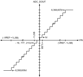 Figure 73. ADC_DOUT vs. VIN of a 24-Bit Resolution (VREF = 5.5V, Gain = 1).
10.2 Typical Applications
10.2.1 3-Wire RTD Using 2 Current Sources
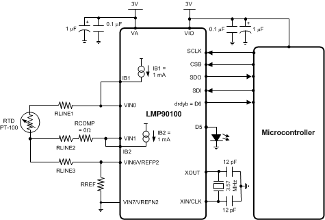 Figure 74. Topology 1: 3-Wire RTD Using 2 Current Sources
10.2.1.1 Design Requirements
- VA = 3V
- VIO = 3V
- 3-Wire RTD using 2 current sources
10.2.1.2 Detailed Design Procedure
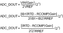
Figure 74 shows the first topology for a 3-wire resistive temperature detector (RTD) application. Topology 1 uses two excitation current sources, IB1 and IB2, to create a differential voltage across VIN0 and VIN1. As a result of using both IB1 and IB2, only one channel (VIN0-VIN1) needs to be measured. As shown in Equation 14, the equation for this channel is IB1 x (RTD – RCOMP) assuming that RLINE1 = RLINE2. Equation 14 is the VIN equation for Topology 1.

The PT-100 changes linearly from 100Ω at 0°C to 146.07Ω at 120°C. If desired, choose a suitable compensating resistor (RCOMP) so that VIN can be virtually 0V at any desirable temperature. For example, if RCOMP = 100Ω, then at 0°C, VIN = 0V and thus a higher gain can be used.
The advantage of this circuit is its ratiometric configuration, where VREF = (IB1 + IB2) x (RREF). Equation 15 shows that a ratiometric configuration eliminates IB1 and IB2 from the output equation, thus increasing the overall performance. Equation 15 is for ADC_DOUT showing IB1 and IB2 eimination.
10.2.1.3 Application Curve
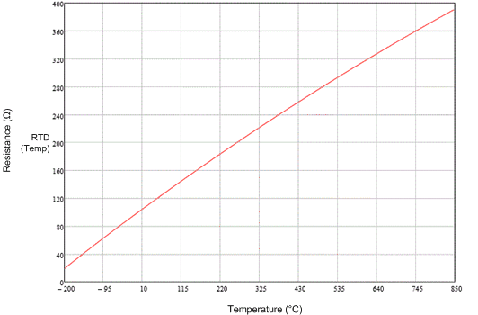 Figure 75. PT-100 RTD Resistance from –200°C to 850°C
10.2.2 3-Wire RTD Using 1 Current Source
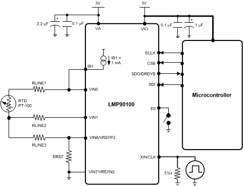 Figure 76. Topology 2: 3-Wire RTD Using 1 Current Source
10.2.2.1 Design Requirements
- VA = 3V
- VIO = 3V
- 3-Wire RTD using 1 current source
10.2.2.2 Detailed Design Procedure
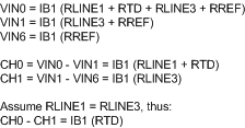
Figure 76 shows the second topology for a 3-wire RTD application. Topology 2 shows the same connection as topology 1, but without IB2. Although this topology eliminates a current source, it requires two channel measurements as shown in Equation 4.
10.2.2.3 Application Curve
 Figure 77. PT-100 RTD Resistance from –200°C to 850°C
10.2.3 Thermocouple with Cold Junction Compensation
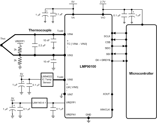 Figure 78. Thermocouple With CJC
10.2.3.1 Design Requirements
- VA = 5V
- VIO = 2.7V
- Thermocouple with Cold Junction Compensation
10.2.3.2 Detailed Design Procedure
The LMP90xxx is also ideal for thermocouple temperature applications. Thermocouples have several advantages that make them popular in many industrial and medical applications. Compare to RTDs, thermistors, and IC sensors, thermocouples are the most rugged, least expensive, and can operate over the largest temperature range.
A thermocouple is a sensor whose junction generates a differential voltage, VIN, that is relative to the temperature difference (Thot – Tcold). Thot is also known as the measuring junction or “hot” junction, which is placed at the measured environment. Tcold is also known as the reference or “cold” junction, which is placed at the measuring system environment.
Because a thermocouple can only measure a temperature difference, it does not have the ability to measure absolute temperature. To determine the absolute temperature of the measured environment (Thot), a technique known as cold junction compensation (CJC) must be used.
In a CJC technique, the “cold” junction temperature, Tcold, is sensed by using an IC temperature sensor, such as the LM94022. The temperature sensor should be placed within close proximity of the reference junction and should have an isothermal connection to the board to minimize any potential temperature gradients.
Once Tcold is obtained, use a standard thermocouple look-up-table to find its equivalent voltage. Next, measure the differential thermocouple voltage and add the equivalent cold junction voltage. Lastly, convert the resulting voltage to temperature using a standard thermocouple look-up-table.
For example, assume Tcold = 20°C. The equivalent voltage from a type K thermocouple look-up-table is 0.798 mV. Next, add the measured differential thermocouple voltage to the Tcold equivalent voltage. For example, if the thermocouple voltage is 4.096 mV, the total would be 0.798 mV + 4.096 mV = 4.894 mV. Referring to the type K thermocouple table gives a temperature of 119.37°C for 4.894 mV.
10.2.4 Application Curve
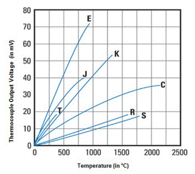 Figure 79. Thermocouple Output as Function of Temperature