ZHCSAU0B April   2012  – October 2015 LMP91002

PRODUCTION DATA.  

  1. 特性
  2. 应用
  3. 说明
  4. 修订历史记录
  5. Pin Configuration and Functions
  6. Specifications
    1. 6.1 Absolute Maximum Ratings
    2. 6.2 ESD Ratings
    3. 6.3 Recommended Operating Conditions
    4. 6.4 Thermal Information
    5. 6.5 Electrical Characteristics
    6. 6.6 I2C Interface
    7. 6.7 Timing Characteristics
    8. 6.8 Typical Characteristics
  7. Detailed Description
    1. 7.1 Overview
    2. 7.2 Functional Block Diagram
    3. 7.3 Feature Description
      1. 7.3.1 Potentiostat Circuitry
      2. 7.3.2 Transimpedance Amplifier
      3. 7.3.3 Control Amplifier
      4. 7.3.4 Internal Zero
      5. 7.3.5 2-Lead Galvanic Cell in Potentiostat Configuration
    4. 7.4 Device Functional Modes
      1. 7.4.1 Timeout Feature
    5. 7.5 Programming
      1. 7.5.1 I2C Interface
      2. 7.5.2 Write and Read Operation
      3. 7.5.3 Connection of More Than One LMP91002 to the I2C Bus
    6. 7.6 Register Maps
      1. 7.6.1 STATUS Register (Offset = 00h)
      2. 7.6.2 LOCK Register (Offset = 01h)
      3. 7.6.3 TIACN Register (Offset = 10h)
      4. 7.6.4 REFCN Register (Offset = 11h)
      5. 7.6.5 MODECN Register (Offset = 12h)
  8. Application and Implementation
    1. 8.1 Application Information
      1. 8.1.1 Gas Sensor Interface
        1. 8.1.1.1 3-Lead Amperometric Cell In Potentiostat Configuration
      2. 8.1.2 Sensor Test Procedure
    2. 8.2 Typical Application
      1. 8.2.1 Design Requirements
      2. 8.2.2 Detailed Design Procedure
        1. 8.2.2.1 Smart Gas Sensor Analog Front End
        2. 8.2.2.2 Smart Gas Sensor AFES on I2C Bus
      3. 8.2.3 Application Curves
  9. Power Supply Recommendations
    1. 9.1 Power Consumption
  10. 10Layout
    1. 10.1 Layout Guidelines
    2. 10.2 Layout Example
  11. 11器件和文档支持
    1. 11.1 社区资源
    2. 11.2 商标
    3. 11.3 静电放电警告
    4. 11.4 Glossary
  12. 12机械、封装和可订购信息

封装选项

机械数据 (封装 | 引脚)
散热焊盘机械数据 (封装 | 引脚)
订购信息

10 Layout

10.1 Layout Guidelines

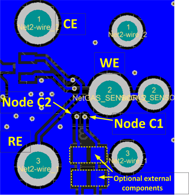
Figure 30 and Figure 31 show an example layout for the LMP91002. Figure 30 shows the top layer, and Figure 31 shows the bottom layer. Figure 30 shows that the sensor electrodes may be arranged around the LMP91002 so that the sensor sets directly over the LMP91002, creating a compact layout. There are very few components needed for the LMP91002: one or more bypass capacitors attached to VDD, and one or two optional external components attached to pins C1 or C2 of the TIA that can provide extra filtering or gain. In the layout shown here, the VDD bypass capacitor is on the top layer, close to the LMP91002, while the optional components for the TIA are placed on the bottom layer. However, these components may also be placed on the top layer.

10.2 Layout Example
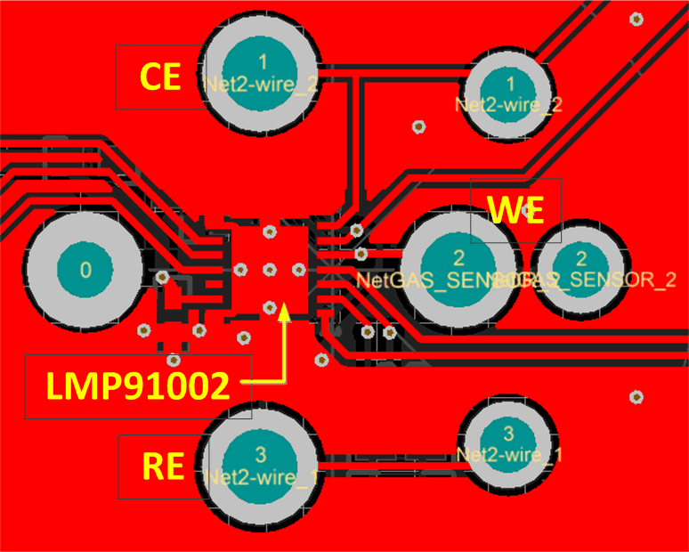
LMP91002 LMP91002_layout_top.gif Figure 30. Layout Example – Top Layer
LMP91002 LMP91002_layout_bot.gif Figure 31. Layout Example – Bottom Layer