SNAS517E November 2011 – September 2015 LMP91050
PRODUCTION DATA.
- 1 Features
- 2 Applications
- 3 Description
- 4 Revision History
- 5 Description (continued)
- 6 Pin Configuration and Functions
- 7 Specifications
- 8 Detailed Description
- 9 Application and Implementation
- 10Power Supply Recommendations
- 11Layout
- 12Device and Documentation Support
- 13Mechanical, Packaging, and Orderable Information
1 Features
- Programmable Gain Amplifier
- Dark Signal Offset Cancellation
- Supports External Filtering
- Common-Mode Generator and 8-Bit DAC
- Key Specifications
- Programmable Gain 167 to 7986 V/V
- Low Noise (0.1 to 10 Hz) 0.1 μVRMS
- Gain Drift 100 ppm/°C (Maximum)
- Phase Delay Drift 500 ns (Maximum)
- Power Supply Voltage Range 2.7 to 5.5 V
2 Applications
- NDIR Sensing
- Demand Control Ventilation
- Building Monitoring
- CO2 Cabin Control — Automotive
- Alcohol Detection — Automotive
- Industrial Safety and Security
- GHG and Freons Detection Platforms
3 Description
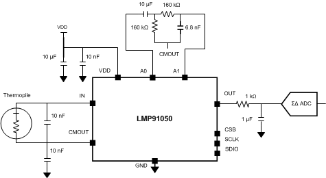
The LMP91050 device is a programmable integrated Sensor Analog Front End (AFE) optimized for thermopile sensors, as typically used in NDIR applications. It provides a complete signal path solution between a sensor and microcontroller that generates an output voltage proportional to the thermopile voltage. The programmability of the LMP91050 enables it to support multiple thermopile sensors with a single design as opposed to the multiple discrete solutions.
The LMP91050 features a programmable gain amplifier (PGA), dark phase offset cancellation, and an adjustable common-mode generator (1.15 V or 2.59 V) which increases output dynamic range. The PGA offers a low-gain range of 167 V/V to 1335 V/V plus a high-gain range of 1002 V/V to 7986 V/V which enables the user to use thermopiles with different sensitivities. The PGA is highlighted by low-gain drift (100 ppm/°C), output offset drift (1.2 mV/°C at G = 1002 V/V), phase delay drift (500 ns) and noise specifications (0.1 μVRMS 0.1 to 10Hz).
Device Information(1)
| PART NUMBER | PACKAGE | BODY SIZE (NOM) |
|---|---|---|
| LMP91050 | VSSOP (10) | 3.00 mm × 3.00 mm |
- For all available packages, see the orderable addendum at the end of the data sheet.
Typical Application Circuit

| Configurable AFE for NDIR |