ZHCSDM8A June 2013 – December 2014 LMP92064
PRODUCTION DATA.
- 1 特性
- 2 应用
- 3 说明
- 4 修订历史记录
- 5 Pin Configuration and Functions
- 6 Specifications
- 7 Detailed Description
- 8 Application and Implementation
- 9 Power Supply Recommendations
- 10Layout
- 11器件和文档支持
- 12机械、封装和可订购信息
6 Specifications
6.1 Absolute Maximum Ratings(2)
over operating free-air temperature range (unless otherwise noted)(1)| MIN | MAX | UNIT | ||
|---|---|---|---|---|
| Analog Supply Voltage (VDD) | –0.3 | 6.0 | V | |
| Digital Supply Voltage (VDIG) | VDD-0.3 | VDD+0.3 | ||
| Voltage at Input Pins(3) | –0.3 | VDD+0.3 | V | |
| Junction Temperature | 150 | °C | ||
| Mounting temperature | Infrared or convection (20 sec) | 260 | °C | |
| Storage temperature, Tstg | −65 | 150 | °C | |
(1) Stresses beyond those listed under Absolute Maximum Ratingsmay cause permanent damage to the device. These are stress ratings only, which do not imply functional operation of the device at these or any other conditions beyond those indicated under Recommended Operating Conditions. Exposure to absolute-maximum-rated conditions for extended periods may affect device reliability.
(2) All voltages are measured with respect to GND = DGND = 0 V, unless otherwise specified.
(3) When the input voltage (VIN), at any pin exceeds power supplies (VIN < GND or VIN > VDD), the current at that pin must not exceed 5 mA, and the voltage (VIN) at that pin must not exceed 6.0 V. See Pin Description for additional details of input circuitry.
6.2 ESD Ratings
| VALUE | UNIT | |||
|---|---|---|---|---|
| V(ESD) | Electrostatic discharge | Human-body model (HBM), per ANSI/ESDA/JEDEC JS-001(1) | ±2000 | V |
| Charged-device model (CDM), per JEDEC specification JESD22-C101(2) | ±1000 | |||
(1) JEDEC document JEP155 states that 500-V HBM allows safe manufacturing with a standard ESD control process.
(2) JEDEC document JEP157 states that 250-V CDM allows safe manufacturing with a standard ESD control process.
6.3 Recommended Operating Conditions(1)
over operating free-air temperature range (unless otherwise noted)| MIN | MAX | UNIT | ||
|---|---|---|---|---|
| Analog Supply Voltage (VDD) | 4.5 | 5.5 | V | |
| Digital Supply Voltage (VDIG) | VDD | VDD | V | |
| Temperature Range | –40 | 105 | ºC | |
(1) All voltages are measured with respect to GND = DGND = 0 V, unless otherwise specified.
6.4 Thermal Information
Over operating free-air temperature range (unless otherwise noted)| THERMAL METRIC(1) | LMP92064 | UNIT | |
|---|---|---|---|
| NHR | |||
| 16 PINS | |||
| RθJA | Package thermal resistance(2) | 44 | °C/W |
(1) For more information about traditional and new thermal metrics, see the IC Package Thermal Metrics application report, SPRA953.
(2) The package thermal impedance is calculated in accordance with JESD 51-7. The maximum power dissipation must be de-rated at elevated temperatures and is dictated by TJ(MAX) , θ JA, and the ambient temperature, TA. The maximum allowable power dissipation PDMAX = (TJ(MAX) - TA )/ θJA or the number given in Absolute Maximum Ratings, whichever is lower.
6.5 Electrical Characteristics
Typical specifications are at 25ºC. All specifications are at 4.5 V ≤ VDD ≤ 5.5 V, VDIG = VDD and –0.2 V ≤ VCM ≤ 2 V, unless otherwise specified.| PARAMETER | TEST CONDITIONS | MIN | TYP | MAX | UNIT | |
|---|---|---|---|---|---|---|
| CURRENT SENSE INPUT CHANNEL | ||||||
| VOS | Input-referred Offset Voltage | ±15 | μV | |||
| Temperature extremes | -60 | 60 | ||||
| TCVOS | Input-referred Offset Voltage Drift | ±280 | nV/ºC | |||
| Long-term Stability | 0.3 | μV/mo | ||||
| Resolution | 12 20 |
Bits μV |
||||
| INL | Integral Non-Linearity Error | ±1% ±0.025% |
LSB |
|||
| DNL | Differential Non-Linearity Error | ±0.5 | LSB | |||
| DC CMRR | Common-Mode Rejection Ratio | –0.2 V ≤ VCM ≤ 2 V | 110 | dB | ||
| DC PSRR | Power Supply Rejection Ratio | 4.5 V ≤ VDD ≤ 5.5 V | 100 | dB | ||
| CMVR | Common-Mode Voltage Range | Low VCM | –0.2 | V | ||
| High VCM | 2 | |||||
| VDIFF(MAX) | Maximum Differential Input Voltage Range | 75 | mV | |||
| AV | Current Shunt Amplifier Gain | 25 | V/V | |||
| Current Sense Channel Gain | 50 | kCode/V | ||||
| GE | Gain Error (CSA, VREF and ADC) | Temperature extremes | -0.75% | 0.75 % | ||
| GD | Gain Drift | ±25 | ppm/°C | |||
| RIN | Input Impedance | 100 | GΩ | |||
| BW | –3dB Bandwidth | 70 | kHz | |||
| VOLTAGE INPUT CHANNEL | ||||||
| Offset Error (Buffer and ADC) | Temperature extremes | -2 | 2 | mV | ||
| Resolution | 12 | Bits | ||||
| INL | Integral Non-Linearity Error | ±1% ±0.025% |
LSB |
|||
| DC PSRR | Power Supply Rejection Ratio | 70 | dB | |||
| VCHVP | Full-Scale Input Voltage | 2.048 | V | |||
| AV | Buffer Amplifier Gain | 1 | V/V | |||
| Voltage Sense Channel Gain | 2 | kCode/V | ||||
| GE | Gain Error (Buffer, VREF and ADC) | Temperature extremes | -0.75% | 0.75 % | ||
| RIN | Input Impedance | 100 | GΩ | |||
| BW | Bandwidth(1) | 100 | kHz | |||
| DIGITAL INPUT/OUTPUT CHARACTERISTICS | ||||||
| VIH | Logical “1” Input Voltage | Temperature extreme | 0.7*VDIG | V | ||
| VIL | Logical “0” Input Voltage | Temperature extreme | 0.3*VDIG | V | ||
| VOH | Logical “1” Output Voltage | ISOURCE = 300 μA | V | |||
| Temperature extreme | VDIG –0.15 |
|||||
| VOL | Logical “0” Output Voltage | ISINK = 300 μA | V | |||
| Temperature extreme | DGND +0.15 |
|||||
| SUPPLY CHARACTERISTICS | ||||||
| IVDD | Analog Supply Current | 11 | mA | |||
| IVDIG | Digital Supply Current | 2 | mA | |||
(1) No analog filter; limited by sampling rate.
6.6 Timing Requirements
Typical specifications are at 25ºC. All specifications are at 4.5 V ≤ VDD ≤ 5.5 V, VDIG = VDD and a 20 pF capacitive load on SDO, unless otherwise specified.| MIN | MAX | UNIT | ||
|---|---|---|---|---|
| tDS | SDI to SCLK rising edge setup time | 10 | ns | |
| tDH | SCLK rising edge to SDI hold time | 10 | ns | |
| fCLK | Frequency of SCLK | 100 | Hz | |
| 20 | MHz | |||
| tHIGH | High width of SPI clock | 25 | ns | |
| tLOW | Low width of SPI clock | 25 | ns | |
| tS | CSB falling edge to SCLK rising edge setup time | 10 | ns | |
| tC | SCLK rising edge to CSB rising edge hold time | 30 | ns | |
| tDV | SCLK falling edge to valid SDO readback data | 20 | ns | |
| tRST | Reset pin pulse width | 3.5 | ns | |
| tCONV | Conversion rate of all channels | 125 | kSps | |
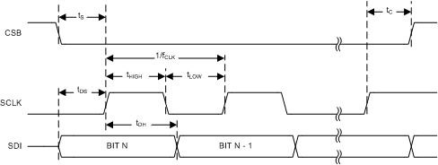 Figure 1. Serial Control Port Timing – Write
 Figure 2. Serial Control Port Timing – Read
 Figure 3. Serial Control Port Write – MSB First, 16-Bit Instruction, Timing Measurements
6.7 Typical Characteristics
All plots at TA = 25ºC, VDD = 5.0 V, VDIG = 5.0 V, VCM = 0 V and GND = DGND = 0 V, unless otherwise specified.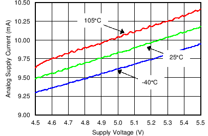 Figure 4. Analog Supply Current vs Supply Voltage
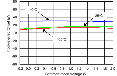 Figure 6. Input-Referred Offset Vscommon-Mode Voltage (Current Channel)
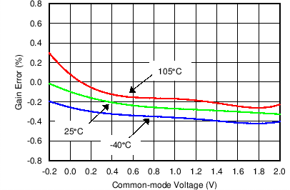 Figure 8. Gain Error vs Common-Mode Voltage (Current Channel)
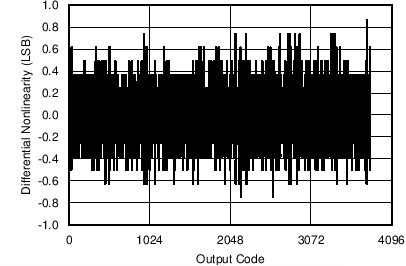 Figure 10. Differential Nonlinearity (Current Channel)
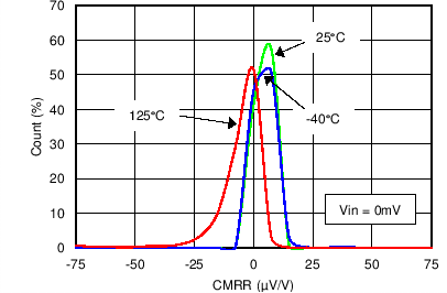 Figure 12. Common-Mode Rejection Ratio Distribution (Current Channel)
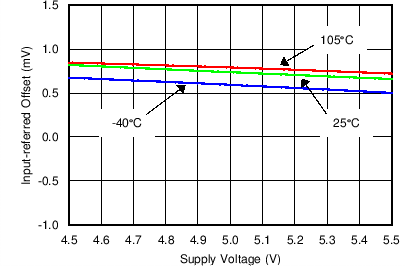 Figure 14. Input-Referred Offset Vssupply Voltage (Voltage Channel)
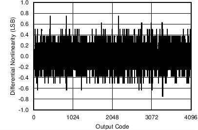 Figure 16. Differential Nonlinearity (Voltage Channel)
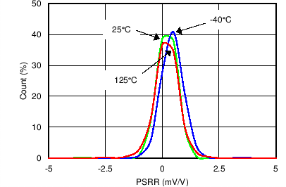 Figure 18. Power Supply Rejection Ratio Distribution (Voltage Channel)
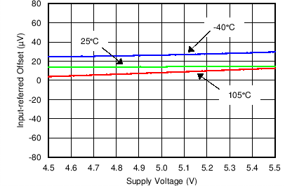 Figure 5. Input-Referred Offset vs Supply Voltage (Current Channel)
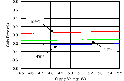 Figure 7. Gain Error vs Supply Voltage (Current Channel)
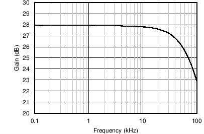 Figure 9. Gain Vsfrequency (Current Channel)
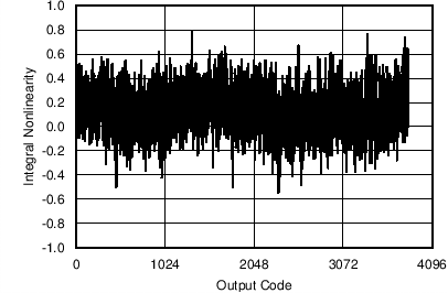 Figure 11. Integral Nonlinearity (Current Channel)
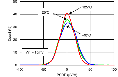 Figure 13. Power Supply Rejection Ratio Distribution Vcm = -0.2 V (Current Channel)
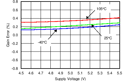 Figure 15. Gain Error vs Supply Voltage (Voltage Channel)
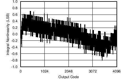 Figure 17. Integral Nonlinearity (Voltage Channel)
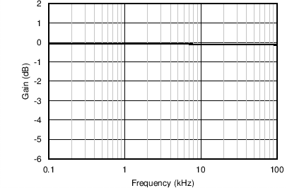 Figure 19. Gain vs Frequency (Voltage Channel)