ZHCSJY0B June 2012 – June 2019 LMR12015 , LMR12020
PRODUCTION DATA.
- 1 特性
- 2 应用
- 3 说明
- 4 修订历史记录
- 5 Pin Configuration and Functions
- 6 Specifications
- 7 Detailed Description
-
8 Application and Implementation
- 8.1 Application Information
- 8.2
Typical Application
- 8.2.1
Detailed Design Procedure
- 8.2.1.1 Custom Design With WEBENCH® Tools
- 8.2.1.2 Inductor Selection
- 8.2.1.3 Input Capacitor
- 8.2.1.4 Output Capacitor
- 8.2.1.5 Catch Diode
- 8.2.1.6 Boost Diode (Optional)
- 8.2.1.7 Boost Capacitor
- 8.2.1.8 Output Voltage
- 8.2.1.9 Feedforward Capacitor (Optional)
- 8.2.1.10
Calculating Efficiency and Junction Temperature
- 8.2.1.10.1 Schottky Diode Conduction Losses
- 8.2.1.10.2 Inductor Conduction Losses
- 8.2.1.10.3 MOSFET Conduction Losses
- 8.2.1.10.4 MOSFET Switching Losses
- 8.2.1.10.5 IC Quiescent Losses
- 8.2.1.10.6 MOSFET Driver Losses
- 8.2.1.10.7 Total Power Losses
- 8.2.1.10.8 Efficiency Calculation Example
- 8.2.1.10.9 Calculating the LMR2015/20 Junction Temperature
- 8.2.2 Application Curves
- 8.2.3 LMR12015/20 Circuit Examples
- 8.2.1
Detailed Design Procedure
- 9 Layout
- 10器件和文档支持
- 11机械、封装和可订购信息
7.3.2 Low Input Voltage Considerations
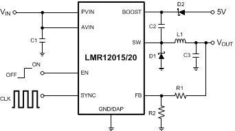
When the input voltage is below 5V and the duty cycle is greater than 75 percent, the gate drive voltage developed across CBOOST might not be sufficient for proper operation of the NMOS switch. In this case, CBOOST should be charged via an external Schottky diode attached to a 5-V voltage rail, see Figure 23. This ensures that the gate drive voltage is high enough for proper operation of the NMOS switch in the triode region. Maintain VBOOST – VSW less than the 6-V absolute maximum rating.
 Figure 23. External Diode Charges CBOOST