ZHCSJY0B June 2012 – June 2019 LMR12015 , LMR12020
PRODUCTION DATA.
- 1 特性
- 2 应用
- 3 说明
- 4 修订历史记录
- 5 Pin Configuration and Functions
- 6 Specifications
- 7 Detailed Description
-
8 Application and Implementation
- 8.1 Application Information
- 8.2
Typical Application
- 8.2.1
Detailed Design Procedure
- 8.2.1.1 Custom Design With WEBENCH® Tools
- 8.2.1.2 Inductor Selection
- 8.2.1.3 Input Capacitor
- 8.2.1.4 Output Capacitor
- 8.2.1.5 Catch Diode
- 8.2.1.6 Boost Diode (Optional)
- 8.2.1.7 Boost Capacitor
- 8.2.1.8 Output Voltage
- 8.2.1.9 Feedforward Capacitor (Optional)
- 8.2.1.10
Calculating Efficiency and Junction Temperature
- 8.2.1.10.1 Schottky Diode Conduction Losses
- 8.2.1.10.2 Inductor Conduction Losses
- 8.2.1.10.3 MOSFET Conduction Losses
- 8.2.1.10.4 MOSFET Switching Losses
- 8.2.1.10.5 IC Quiescent Losses
- 8.2.1.10.6 MOSFET Driver Losses
- 8.2.1.10.7 Total Power Losses
- 8.2.1.10.8 Efficiency Calculation Example
- 8.2.1.10.9 Calculating the LMR2015/20 Junction Temperature
- 8.2.2 Application Curves
- 8.2.3 LMR12015/20 Circuit Examples
- 8.2.1
Detailed Design Procedure
- 9 Layout
- 10器件和文档支持
- 11机械、封装和可订购信息
9.1.1 Compact Layout
The performance of any switching converter depends as much upon the layout of the PCB as the component selection. The following guidelines will help the user design a circuit with maximum rejection of outside EMI and minimum generation of unwanted EMI.
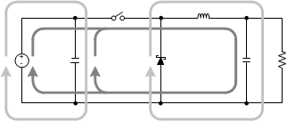
Parasitic inductance can be reduced by keeping the power path components close together and keeping the area of the loops small, on which high currents travel. Short, thick traces or copper pours (shapes) are best. In particular, the switch node (where L1, D1, and the SW pin connect) should be just large enough to connect all three components without excessive heating from the current it carries. The LMR12015/20 operates in two distinct cycles (see Figure 22) whose high current paths are shown below in Figure 43:
 Figure 43. Buck Converter Current Loops
 The dark grey, inner loop represents the high current path during the MOSFET on-time. The light grey, outer loop represents the high current path during the off-time.