ZHCSF39A November 2015 – February 2016 LMR14050-Q1
PRODUCTION DATA.
- 1 特性
- 2 应用范围
- 3 说明
- 4 修订历史记录
- 5 Pin Configuration and Functions
- 6 Specifications
-
7 Detailed Description
- 7.1 Overview
- 7.2 Functional Block Diagram
- 7.3
Feature Description
- 7.3.1 Fixed Frequency Peak Current Mode Control
- 7.3.2 Slope Compensation
- 7.3.3 Sleep-mode
- 7.3.4 Low Dropout Operation and Bootstrap Voltage (BOOT)
- 7.3.5 Adjustable Output Voltage
- 7.3.6 Enable and Adjustable Under-voltage Lockout
- 7.3.7 External Soft-start
- 7.3.8 Switching Frequency and Synchronization (RT/SYNC)
- 7.3.9 Power Good (PGOOD)
- 7.3.10 Over Current and Short Circuit Protection
- 7.3.11 Overvoltage Protection
- 7.3.12 Thermal Shutdown
- 7.4 Device Functional Modes
- 8 Application and Implementation
- 9 Power Supply Recommendations
- 10Layout
- 11器件和文档支持
- 12机械、封装和可订购信息
封装选项
机械数据 (封装 | 引脚)
散热焊盘机械数据 (封装 | 引脚)
- DDA|8
订购信息
6 Specifications
6.1 Absolute Maximum Ratings
Over the recommended operating junction temperature range of -40 °C to 125 °C (unless otherwise noted) (1)(1) Stresses beyond those listed under Absolute Maximum Ratings may cause permanent damage to the device. These are stress ratings only, which do not imply functional operation of the device at these or any other conditions beyond those indicated under Recommended Operating Conditions. Exposure to absolute-maximum-rated conditions for extended periods may affect device reliability.
6.2 ESD Ratings
| VALUE | UNIT | |||
|---|---|---|---|---|
| V(ESD) | Electrostatic discharge | Human-body model (HBM), per AEC Q100-002 (1) | ±2000 | V |
| Charged-device model (CDM), per AEC Q100-011 | ±750 | |||
(1) AEC Q100-002 indicates that HBM stressing shall be in accordance with the ANSI/ESDA/JEDEC JS-001 specification.
6.3 Recommended Operating Conditions
Over the recommended operating junction temperature range of -40 °C to 125 °C (unless otherwise noted) (1)(1) Operating Ratings indicate conditions for which the device is intended to be functional, but do not guarantee specific performance limits. For guaranteed specifications, see Electrical Characteristics .
6.4 Thermal Information
| THERMAL METRIC (1) (2) | LMR14050-Q1 | UNIT | |
|---|---|---|---|
| DDA (HSOIC) | |||
| 8 PINS | |||
| RθJA | Junction-to-ambient thermal resistance | 42.5 | °C/W |
| ψJT | Junction-to-top characterization parameter | 9.9 | °C/W |
| ψJB | Junction-to-board characterization parameter | 25.4 | °C/W |
| RθJC(top) | Junction-to-case (top) thermal resistance | 56.1 | °C/W |
| RθJC(bot) | Junction-to-case (bottom) thermal resistance | 3.8 | °C/W |
| RθJB | Junction-to-board thermal resistance | 25.5 | °C/W |
(1) For more information about traditional and new thermal metrics, see the Semiconductor and IC Package Thermal Metrics application report, SPRA953.
(2) Power rating at a specific ambient temperature TA should be determined with a maximum junction temperature (TJ) of 125°C, which is illustrated in Recommended Operating Conditions section.
6.5 Electrical Characteristics
Limits apply over the recommended operating junction temperature (TJ) range of -40°C to +125°C, unless otherwise stated. Minimum and Maximum limits are specified through test, design or statistical correlation. Typical values represent the most likely parametric norm at TJ = 25°C, and are provided for reference purposes only. Unless otherwise specified, the following conditions apply: VIN = 4.0 V to 40 V6.6 Switching Characteristics
Over the recommended operating junction temperature range of -40 °C to 125 °C (unless otherwise noted)| PARAMETER | TEST CONDITIONS | MIN | TYP | MAX | UNIT | |
|---|---|---|---|---|---|---|
| fSW | Switching frequency | RT = 11.5 kΩ | 1758 | 1912 | 2066 | kHz |
| Switching frequency range at SYNC mode | 250 | 2300 | ||||
| FDITHER | Switching frequency dithering | Spread spectrum option, frequency dithering over center frequency | ±6% | |||
| VSYNC_HI | SYNC clock high level threshold | 1.7 | V | |||
| VSYNC_LO | SYNC clock low level threshold | 0.5 | ||||
| TSYNC_MIN | Minimum SYNC input pulse width | Measured at 500 kHz, VSYNC_HI > 3 V, VSYNC_LO < 0.3 V | 30 | ns | ||
| TLOCK_IN | PLL lock in time | Measured at 500 kHz | 100 | µs | ||
| TON_MIN | Minimum controllable on time | VIN = 12 V, BOOT to SW = 5.8 V, ILoad = 1 A | 75 | ns | ||
| DMAX | Maximum duty cycle | fSW = 200 kHz | 97% | |||
6.7 Typical Characteristics
Unless otherwise specified the following conditions apply: VIN = 12 V, fSW = 300 kHz, L = 6.5 µH, COUT = 47 µF x 4, TA = 25°C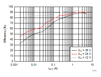
| VOUT = 5 V | fSW = 300 kHz |
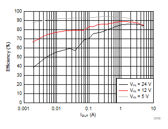
| VOUT = 3.3 V | fSW = 300 kHz |
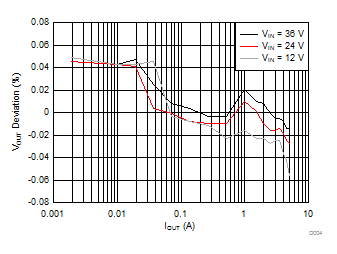
| VOUT = 5 V | fSW = 300 kHz |
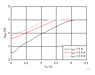
| VOUT = 5 V | fSW = 300 kHz |
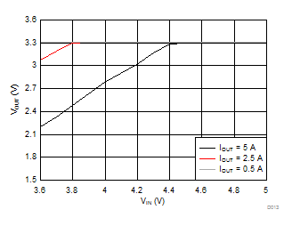
| VOUT = 3.3 V | fSW = 300 kHz |
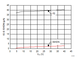

| VOUT = 5 V | fSW = 500 kHz |
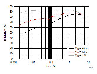
| VOUT = 3.3 V | fSW = 500 kHz |
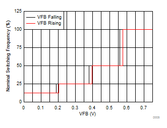
| VOUT = 5 V | fSW = 300 kHz |
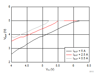
| VOUT = 5V | fSW = 500 KHz |
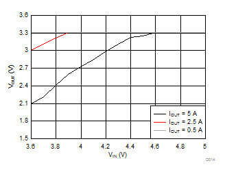
| VOUT = 3.3 V | fSW = 500 kHz |
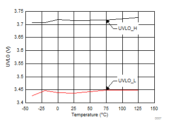
| IOUT = 0 A |