ZHCSDH4A February 2015 – March 2015 LMR14050
PRODUCTION DATA.
- 1 特性
- 2 应用范围
- 3 说明
- 4 简化电路原理图
- 5 修订历史记录
- 6 Pin Configuration and Functions
- 7 Specifications
-
8 Detailed Description
- 8.1 Overview
- 8.2 Functional Block Diagram
- 8.3
Feature Description
- 8.3.1 Fixed Frequency Peak Current Mode Control
- 8.3.2 Slope Compensation
- 8.3.3 Sleep-mode
- 8.3.4 Low Dropout Operation and Bootstrap Voltage (BOOT)
- 8.3.5 Adjustable Output Voltage
- 8.3.6 Enable and Adjustable Under-voltage Lockout
- 8.3.7 External Soft-start
- 8.3.8 Switching Frequency and Synchronization (RT/SYNC)
- 8.3.9 Over Current and Short Circuit Protection
- 8.3.10 Overvoltage Protection
- 8.3.11 Thermal Shutdown
- 9 Application and Implementation
- 10Power Supply Recommendations
- 11Layout
- 12器件和文档支持
- 13机械封装和可订购信息
11 Layout
11.1 Layout Guidelines
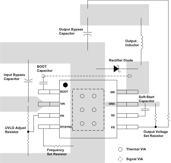
Layout is a critical portion of good power supply design. The following guidelines will help users design a PCB with the best power conversion performance, thermal performance, and minimized generation of unwanted EMI.
- The feedback network, resistor RFBT and RFBB, should be kept close to the FB pin. VOUT sense path away from noisy nodes and preferably through a layer on the other side of a shielding layer .
- The input bypass capacitor CIN must be placed as close as possible to the VIN pin and ground. Grounding for both the input and output capacitors should consist of localized top side planes that connect to the GND pin and PAD .
- The inductor L should be placed close to the SW pin to reduce magnetic and electrostatic noise.
- The output capacitor, COUT should be placed close to the junction of L and the diode D. The L, D, and COUT trace should be as short as possible to reduce conducted and radiated noise and increase overall efficiency.
- The ground connection for the diode, CIN, and COUT should be as small as possible and tied to the system ground plane in only one spot (preferably at the COUT ground point) to minimize conducted noise in the system ground plane
- For more detail on switching power supply layout considerations see Application Note AN-1149
11.2 Layout Example
 Figure 30. Layout