ZHCSDV3 June 2015 LMR16006Y-Q1
PRODUCTION DATA.
- 1 特性
- 2 应用范围
- 3 说明
- 4 简化电路原理图
- 5 修订历史记录
- 6 Pin Configuration and Functions
- 7 Specifications
- 8 Detailed Description
- 9 Application and Implementation
- 10Power Supply Recommendations
- 11Layout
- 12器件和文档支持
- 13机械、封装和可订购信息
7 Specifications
7.1 Absolute Maximum Ratings (1)
| MIN | MAX | UNIT | ||
|---|---|---|---|---|
| Input voltages | VIN to GND | -0.3 | 65 | V |
| SHDN to GND | -0.3 | 65 | ||
| FB to GND | -0.3 | 7 | ||
| CB to SW | -0.3 | 7 | ||
| Output voltages | SW to GND | -1 | 60 | |
| SW to GND less than 30 ns transients | -2 | 60 | ||
| TJ Operation junction temperature | -40 | 150 | °C | |
| Storage temperature, Tstg | -55 | 165 | °C | |
(1) Stresses beyond those listed under Absolute Maximum Ratings may cause permanent damage to the device. These are stress ratings only, which do not imply functional operation of the device at these or any other conditions beyond those indicated under Recommended Operating Conditions. Exposure to absolute-maximum-rated conditions for extended periods may affect device reliability.
7.2 ESD Ratings
| VALUE | UNIT | |||
|---|---|---|---|---|
| V(ESD) | Electrostatic discharge | Human-body model (HBM), per AEC Q100-002(1) | ±2000 | V |
| Charged-device model (CDM), per AEC Q100-011 | ±500 | |||
(1) AEC Q100-002 indicates that HBM stressing shall be in accordance with the ANSI/ESDA/JEDEC JS-001 specification.
7.3 Recommended Operating Conditions
over operating free-air temperature range (unless otherwise noted) (1)| MIN | MAX | UNIT | ||
|---|---|---|---|---|
| Buck regulator | VIN | 4 | 40 | V |
| CB | 4 | 46 | ||
| CB to SW | -0.3 | 6 | ||
| SW | -1 | 40 | ||
| FB | 0 | 5.5 | ||
| Control | SHDN | 0 | 40 | |
| Temperature | Operating junction temperature range, TJ | -40 | 125 | °C |
7.4 Thermal Information
over operating free-air temperature range (unless otherwise noted)| THERMAL METRIC (1) | LMR16006Y-Q1 | UNIT | |
|---|---|---|---|
| DDC (SOT) | |||
| (6 PINS) | |||
| RθJA | Junction-to-ambient thermal resistance | 102 | °C/W |
| RθJCtop | Junction-to-case (top) thermal resistance | 36.9 | |
| RθJB | Junction-to board characterization parameter | 28.4 | |
(1) All numbers apply for packages soldered directly onto a 3" x 3" PC board with 2 oz. copper on 4 layers in still air in accordance to JEDEC standards. Thermal resistance varies greatly with layout, copper thickness, number of layers in PCB, power distribution, numberof thermal vias, board size, ambient temperature, and air flow.
7.5 Electrical Characteristics
Limits apply over the recommended operating junction temperature (TJ) range of -40°C to +125°C, unless otherwise stated. Minimum and Maximum limits are specified through test, design or statistical correlation. Typical values represent the most likely parametric norm at TJ = 25°C, and are provided for reference purposes only. Unless otherwise specified, the following conditions apply: VIN = SHDN = 12 V.| PARAMETER | TEST CONDITIONS | MIN | TYP | MAX | UNIT | ||
|---|---|---|---|---|---|---|---|
| VIN (INPUT POWER SUPPLY) | |||||||
| VIN | Operating input voltage | 4 | 40 | V | |||
| ISHDN | Shutdown supply current | VEN = 0 V | 1 | 3 | µA | ||
| IQ | Operating quiescent current (non-switching) | no load, VIN = 12 V | 28 | µA | |||
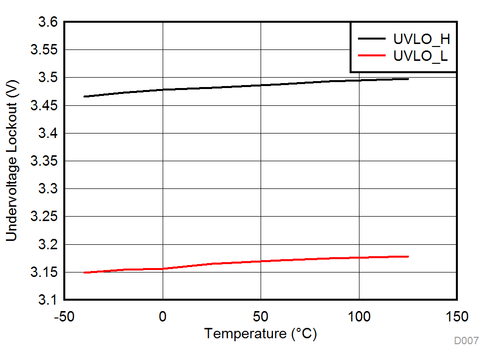
| UVLO | Undervoltage lockout thresholds | Rising threshold | 4 | V | |||
| Falling threshold | 3 | ||||||
| SHDN | |||||||
| VSHDN_Thre | Rising SHDN Threshold Voltage | 1.05 | 1.25 | 1.38 | V | ||
| ISHDN | Input current | SHDN = 2.3 V | -4.2 | µA | |||
| SHDN = 0.9 V | -1 | ||||||
| ISHDN_HYS | Hysteresis current | -3 | µA | ||||
| HIGH-SIDE MOSFET | |||||||
| RDS_ON | On-resistance | VIN = 12 V, CB to SW = 5.8 V | 900 | mΩ | |||
| VOLTAGE REFERENCE (FB PIN) | |||||||
| VFB | Feedback voltage | 0.747 | 0.765 | 0.782 | V | ||
| VOUT | Output voltage | Fixed 3.3 V output version | 3.201 | 3.3 | 3.399 | V | |
| Fixed 5 V output version | 4.85 | 5 | 5.15 | V | |||
| CURRENT LIMIT | |||||||
| ILIMIT | Peak current limit | VIN = 12 V, TJ = 25°C | 1200 | 1700 | mA | ||
| THERMAL PERFORMANCE | |||||||
| TSHDN(1) | Thermal shutdown threshold | 170 | ºC | ||||
| THYS(1) | Hysteresis | 10 | ºC | ||||
(1) Ensured by design.
7.6 Switching Characteristics
over operating free-air temperature range (unless otherwise noted)| PARAMETER | TEST CONDITIONS | MIN | TYP | MAX | UNIT | |
|---|---|---|---|---|---|---|
| SW (SW PIN) | ||||||
| ƒSW | Switching frequency | 1785 | 2100 | 2415 | kHz | |
| TON_MIN(1) | Minimum turn-on time | ƒSW = 2.1 MHz | 80 | ns | ||
| DMAX | Maximum duty cycle | 97% | ||||
(1) Ensured by design.
7.7 Typical Characteristics
Unless otherwise specified the following conditions apply: VIN = 12 V, ƒSW = 2100 kHz, L1 = 6.8 µH, Cout = 10 µF, TA = 25°C.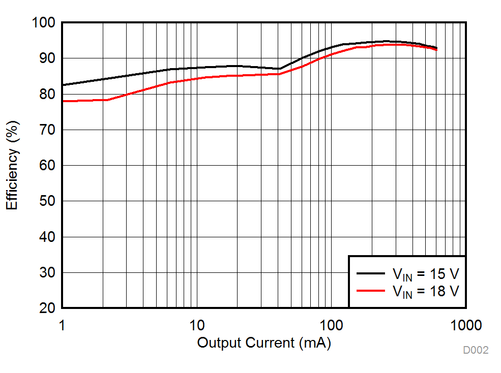
| VOUT = 12 V | ƒSW = 2100 kHz | |
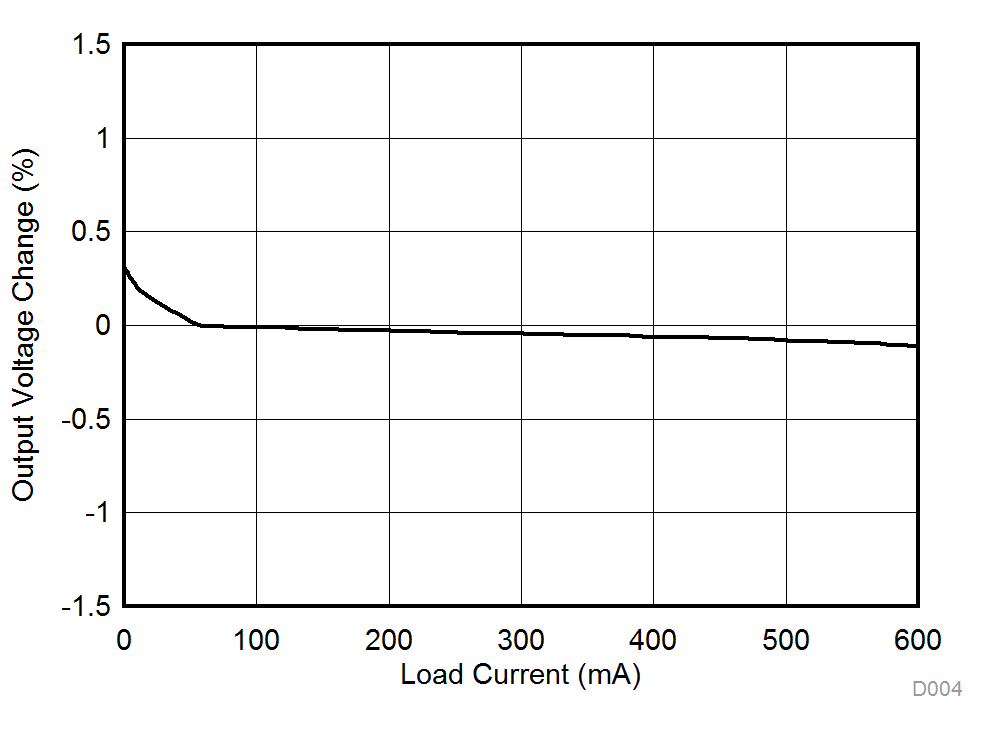
| VOUT = 5 V | ƒSW = 2.1 MHz | |
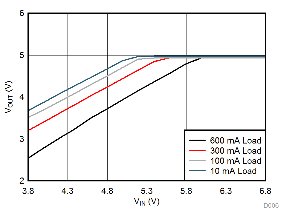
| VOUT = 5 V | ||
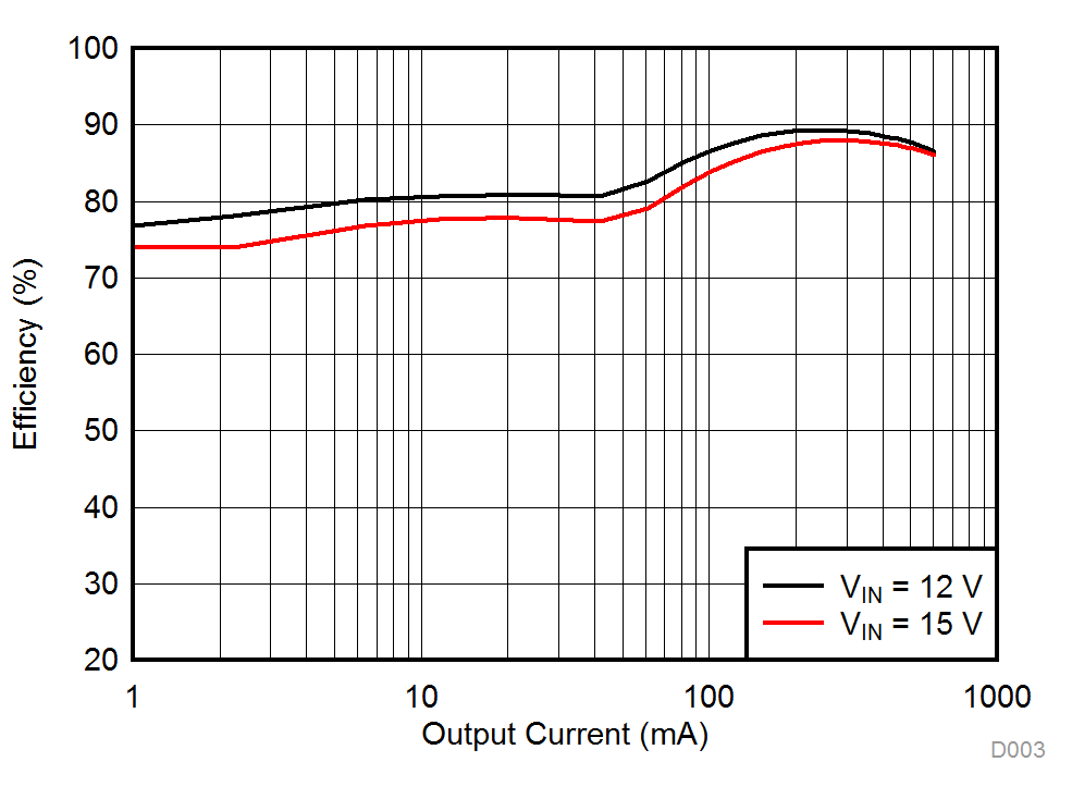
| VOUT = 5 V | ƒSW = 2100 kHz | |
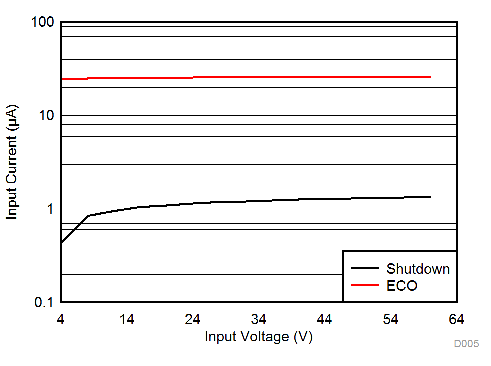
| VOUT = 5 V | ||
