ZHCSFR2B December 2016 – March 2018 LMR23630-Q1
PRODUCTION DATA.
- 1 特性
- 2 应用
- 3 说明
- 4 修订历史记录
- 5 Product Portfolio
- 6 Pin Configuration and Functions
- 7 Specifications
-
8 Detailed Description
- 8.1 Overview
- 8.2 Functional Block Diagram
- 8.3
Feature Description
- 8.3.1 Fixed-Frequency Peak-Current-Mode Control
- 8.3.2 Adjustable Frequency
- 8.3.3 Adjustable Output Voltage
- 8.3.4 Enable/Synchronization
- 8.3.5 VCC, UVLO
- 8.3.6 Minimum ON-time, Minimum OFF-time and Frequency Foldback at Dropout Conditions
- 8.3.7 Power Good (PGOOD)
- 8.3.8 Internal Compensation and CFF
- 8.3.9 Bootstrap Voltage (BOOT)
- 8.3.10 Overcurrent and Short-Circuit Protection
- 8.3.11 Thermal Shutdown
- 8.4 Device Functional Modes
-
9 Application and Implementation
- 9.1 Application Information
- 9.2
Typical Applications
- 9.2.1 Design Requirements
- 9.2.2
Detailed Design Procedure
- 9.2.2.1 Custom Design With WEBENCH® Tools
- 9.2.2.2 Output Voltage Setpoint
- 9.2.2.3 Switching Frequency
- 9.2.2.4 Inductor Selection
- 9.2.2.5 Output Capacitor Selection
- 9.2.2.6 Feed-Forward Capacitor
- 9.2.2.7 Input Capacitor Selection
- 9.2.2.8 Bootstrap Capacitor Selection
- 9.2.2.9 VCC Capacitor Selection
- 9.2.2.10 UVLO Setpoint
- 9.2.3 Application Curves
- 10Power Supply Recommendations
- 11Layout
- 12器件和文档支持
- 13机械、封装和可订购信息
封装选项
机械数据 (封装 | 引脚)
散热焊盘机械数据 (封装 | 引脚)
订购信息
9.2 Typical Applications
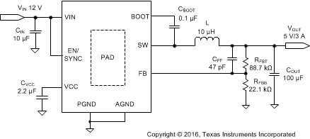
The LMR23630-Q1 only requires a few external components to convert from a wide voltage range supply to a fixed output voltage. Figure 23 shows a basic schematic.
 Figure 23. Application Circuit
The external components have to fulfill the needs of the application, but also the stability criteria of the device control loop. Table 2 can be used to simplify the output filter component selection.
Table 2. L, COUT and CFF Typical Values
| fSW (kHz) | VOUT (V) | L (µH)(1) | COUT (µF)(2) | CFF (pF) | RFBT (kΩ)(3) |
|---|---|---|---|---|---|
| 400 | 3.3 | 6.8 | 150 | 75 | 51 |
| 400 | 5 | 10 | 100 | 47 | 88.7 |
| 400 | 12 | 15 | 68 | See note(4) | 243 |
| 400 | 24 | 15 | 47 | See note(4) | 510 |
(1) Inductance value is calculated based on VIN = 36 V.
(2) All the COUT values are after derating. Add more when using ceramic capacitors.
(3) RFBT = 0 Ω for VOUT = 1 V. RFBB = 22.1 kΩ for all other VOUT setting.
(4) High ESR COUT gives enough phase boost, and CFF not needed.